LOGIN
LOGIN Downloads


The FP Designer allows you to create and/or edit non-standard parts before you auto-generate them.
Any part that is not highly complex and can get started in one of the available calculators
(Surface Mount or Through-hole), you should first use the Calculator, then copy/move the part to FP Designer. start want do do so for two reasons:"
- Save time with most of the part
- 3D STEP models are available for calculator parts (license required)
The most common reason for moving Calculator footprints to FP Designer is to edit the Paste Mask apertures to create a custom paste mask pattern for Thermal Pads.
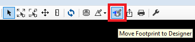
To create a footprint in any Calculator then customize a pad stack, you must move the footprint to FP Designer using the toolbar icon.
There are 5 Calculator component families that cannot be moved to FP designer. These are:
- SMD Capacitor, Aluminum Electrolytic
- SMD DPAK
- PTH TO92
- PTH Flange Mount (TO) Horizontal
- PTH Flange Mount (TO) Vertical
If you need footprints for any of these five types of components, you must manually create them in FP Designer. TIP: Create them in the Calculator, print out the datasheet, and use those dimensions to assist in creating the footprint in FP Designer.
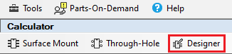
1. FP Designer
Left Mouse Click "Designer"
The first menu to appear is the Body panel that contains "Body", "Options" and "3D STEP Colors".
You first define the Body > Shape "Rectangle" or "Round".
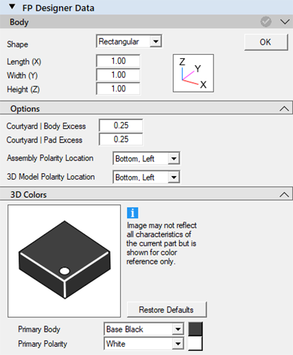
1. Insert the package Nominal - Length & Width and Maximum Height
2. Drop Down the Assembly Polarity Location and select the corner location of Pin 1.
3. Unselect any Outline that you do not want in the final footprint.
4. Add an Assembly Polarity Location and a 3D Model Polarity Location.
a. Upper Left
b. Top Center
c. Upper Right
d. Left Center
e. Right Center
f. Lower Left
g. Bottom Center
h. Lower Right
5. Courtyard Pad Excess
a. Default is 0.25; for microminiature packages can be changed to 0.15
6. Courtyard Body Excess
a. Default is 0.25; for microminiature packages can be changed to 0.15
b. If L, W, or H Dimension is > 10.00, 0.50 is recommended for rework
7. 3D Colors panel allows you to change the Primary Body and Polarity marker
8. Note: all FP Designer 3D Models are extruded using the package dimensions
9. After editing colors in the 3D Colors panel, it is recommended to Close the panel to avoid invoking the scroll bar.
Select the OK button after you insert the package Dimensional Data, Options and 3D STEP Colors.
After the OK button is selected, FP Designer will auto-generate the following PCB library features:
- Legend Outline
- Legend Reference Designator
- Assembly Outline
- Assembly Reference Designator
- Component Body Outline
- Placement Courtyard Outline
- Centroid Origin and Crosshair
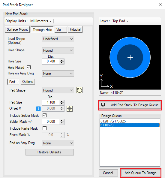
After the OK button is selected, the Green Indicator light for Body will turn on and the Body and Option panels will collapse, and the Pad Stack Designer will automatically open.
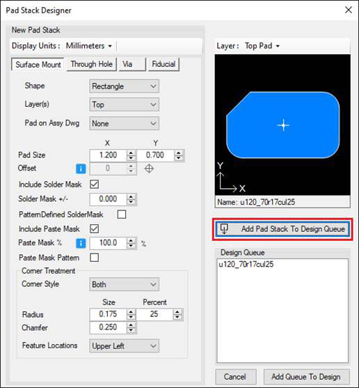
The Pad Stack Designer is primarily used for the creation of new pad stacks. Once the pad stacks are created, the Pad Stack Manager opens to allow you to edit all the layers of the pad stack.
Example: The Pad Stack Designer will create a through-hole pad stack with the same pad size on all layers. But the Pad Stack Manager allows you to edit the pad sizes on the Outer Layers and Inner Layers if you want to make the pad stack unique.
The Pad Stack Manager allows you to add and/or remove layers from your pad stack.
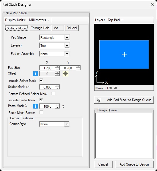
In the Surface Mount pad stack, you can create these pad stacks:
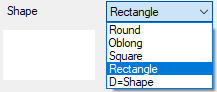
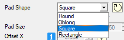
Pad Shape: Round, Oblong, Square, Rectangle and D-Shape
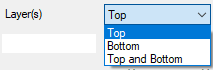
Layers: Top, Bottom, Top & Bottom
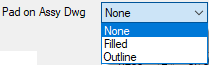
Pad on Assembly Drawing: None, Filled and Outline
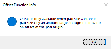
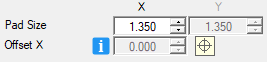
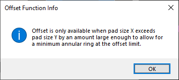
Pad Size: X & Y and Offset
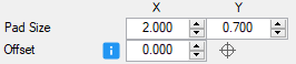
Tech Tip: Click on the blue button: 
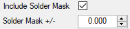
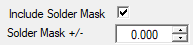
Include Solder Mask and +/- annular over/under size value: Solder Mask Defined or Non-Solder Mask Defined
Pattern Defined Solder Mask: This is used for Thermal Pads to create dams between the Paste Mask patterns.
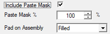
Include Paste Mask: Check box turns paste mask on/off.
Paste Mask %: Default is 100% but Thermal Pad Paste Mask is 50% - 70%.
Paste Mask Pattern: Check box turns on/off a Thermal Pad pattern. On = Checker-Board pattern.
Corner Treatment / Corner Style
- Default is None
- Radius
- Corner Radius Size and Percent options pop up
- Feature Locations: All, Top, Left Top, Bottom
- Chamfer
- Corner Chamfer Size and Percent options pop up
- Feature Locations: All, Top, Left Top, Bottom
- Both
- Feature Locations Radius in 3 corners and Chamfer in one corner
- Any value = 0.00 to turn off feature
When you complete the creation of your pad stack, select "Add Pad Stack to Design Queue".
Through-hole Pad Stack:

In the Through-hole pad stack, you can create these pad stacks:
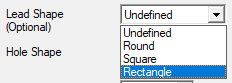
Lead Shape (optional): Undefined, Round Square, Rectangle
If you select a Lead Shape, enter the Maximum Lead Diameter or the Maximum Hypotenuse of the Rectangle
Entering a Lead Diameter will auto-generate the Hole Size per your personal Option setting.
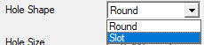
Hole Shape: Round or Slotted
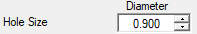
Hole Size: if you do not
enter the terminal lead size, you can insert a hole size. This will
auto-generate the pad size per your personal Option settings.
Hole Plated: this check box will toggle between Plated and Non-plated hole.

Hole on Assembly Drawing: None, Filled and Outline
Pad / Options: Options will display all the default settings:
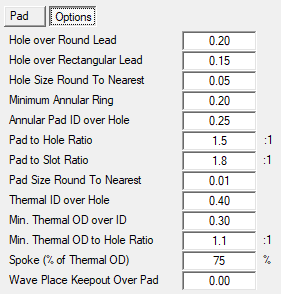
Pad Shape: Round, Oblong, Square, Rectangle. There is a "Recalculate" button next to the pad shape.
Pad Size: Depending on the Shape
- Round will display the Diameter
- Square will display X
- Rectangle will display X & Y
Pad Size: X & Y and Offset
Tech Tip: Click on the blue button
Include Solder Mask and +/- annular over/under size value: Solder Mask Defined or Non-Solder Mask Defined
Include Paste Mask: on/off switch. This is intended for "Pin in Paste technology".
Paste Mask %: is a percentage of the pad size.
Pad on Assembly Drawing: None, Filled and Outline
Thermal Relief on/off - On = pad stack will have a Thermal Relief, Off = the pad stack will not.

When you complete the creation of your pad stack, select "Add Pad Stack to Design Queue".
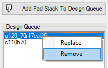
To remove a pad stack from the Queue, select the pad stack and Right Mouse Button > Remove.
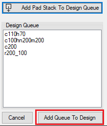
When you finish creating all your pad stacks, select the "Add Queue to Design" button
This will open the Pad Stack Manager to allow you to fully edit all layers of the pad stack.
When pad stack editing is completed, select the "Save and Close" button.
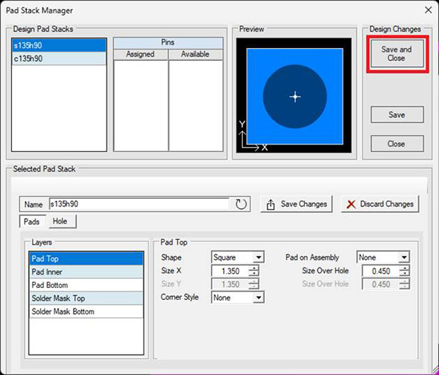
The new pad stacks will be added to the Pad Stack panel and the indicator light will turn Green.
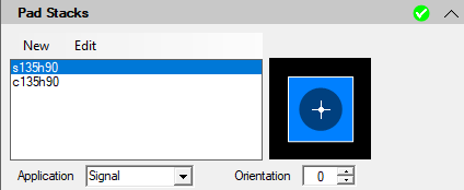
The Application drop down will allow you to change the status of each pad stack.
- Signal
- Mechanical
- Thermal
- Via
- Fiducial
Open the Pad Stack panel to start the creation of your pad stacks by selecting the New button.
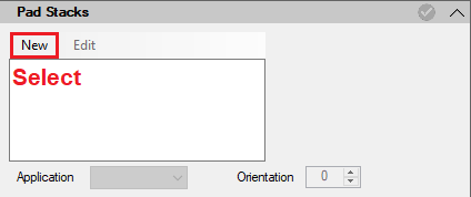
The Pad Stack Designer dialog window will open. You can select Surface Mount, Through-hole or Via.
Next, select the Pins Panel and then the "Define Placement" panel.
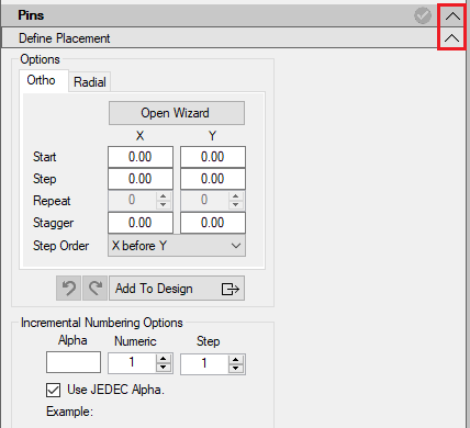
The concept here is to select a pad stack and enter the X, Y coordinates and the Pin Name.
Then select the "Add to Design" button.
If you make a mistake, select the "Undo" button and start over.
When you place the pad stacks, the Green Indicator light will turn on.
To finalize the Footprint, open the Specifications panel.
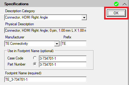
Drop down the Description Category and type in the first 3 characters of the component family and select an option from the list. You can also enter a different component family if the one you need isn't there.
Drop down the Manufacturer and type in the first 3 characters of the manufacturer name and select the correct manufacturer for this footprint. If your manufacturer is not listed, contact PCB Libraries, Inc.
Enter the Case Code from the manufacturer. If the package is a one of a kind and only has one Part Number, enter the part number and select that radio button.
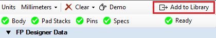
Select the OK button when finished and the Green Indicator light will turn on.
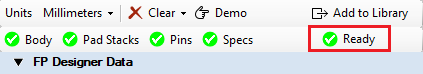
Select the "Finish" button at the top of the FP Designer panels.
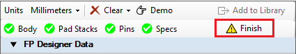
The Finish button will change to "Ready", and the green indicator light will turn on.
Open your FPX file and select the Add to Library button to add the new footprint to the FPX file.