LOGIN
LOGIN Downloads


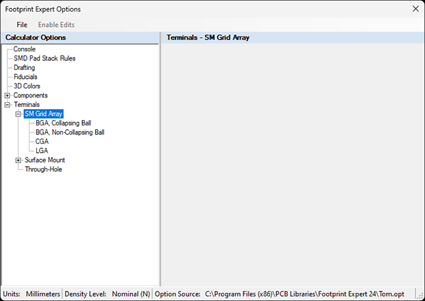
The Terminals options are separated into 3 categories:
- SM Grid Array
- Surface Mount
- Through-hole
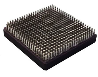
1. SM GRID ARRAY - covers the BGA, CGA & LGA component families.
Terminals options for BGA, Collapsing Ball:
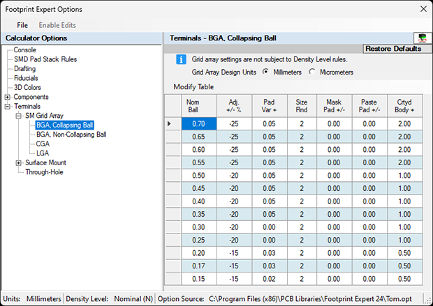
The Collapsing BGA has a table with 7 columns of data which is sorted by the Nominal Ball Diameter.
Nominal Ball Diameter - Footprint Expert comes with 13
nominal ball sizes, but you can add additional Ball size values by Right Mouse
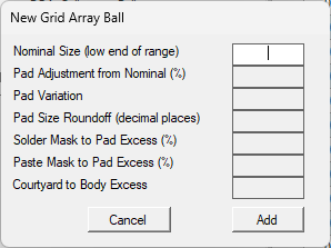
Click anywhere in the table. A dialog box will appear asking to "Insert New
Row". When you select Insert, a dialog box will appear to insert a new
Nominal Ball Size.
The new Ball Size will be automatically sorted by the Ball Diameter and Footprint Expert will add all the column data rules for that density level. You can edit the column data to change the values to whatever you want.
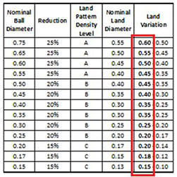
The mathematical model for BGA pad stack calculations includes a Pad Variation tolerance. Once the pad size is calculated, a +/- 0.05 tolerance is added to the pad stack. IPC prefers to use the Maximum Material Condition of the Pad Variation. Example: a 1.00 mm pitch BGA nominal ball size is 0.60. Multiplying 0.60 X 25% = 0.15. 0.60 - 0.15 = 0.45 with a Pad Tolerance of +/- 0.05 = 0.50 max. and 0.40 min. IPC recommends the 0.50 max. pad size. This table is from the IPC-7351 guideline that includes nominal ball diameters in 0.05 increments. The values in the red box indicate the recommended pad size. There are 3-Tiers for BGA pad stack calculations. Nominal ball sizes of 0.55 - 0.75 are the maximum density level "A" with a 25% pad size reduction, 0.25 - 0.50 are the nominal density level "B" with a 20% pad reduction, and 0.15 - 0.20 are the minimum density level "C" with a 15% pad reduction.

Terminals options for BGA, Non-Collapsing Ball:
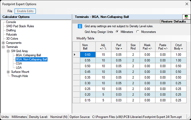
The Non-Collapsing BGA has a table with 7 columns of data which is sorted by the Nominal Ball Diameter.
The Non-Collapsing BGA pad stack features are the same as the Collapsing Balls, but
the calculations are different because rather than pad size reduction, the pad
sizes increase to accommodate solder mask defined pad stacks (used to secure
the pad to the prepreg) or to create an annular ring for drilling holes in the
pad (via in pad technology).
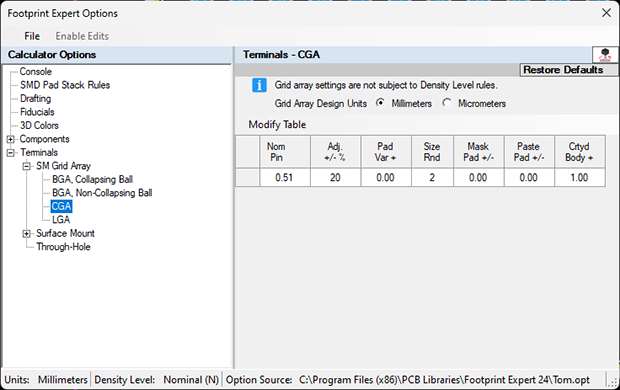
The Column Grid Array (CGA) is setup for you to insert the maximum column terminal
diameters and create the pad size adjustment, Pad Tolerance and Rounding,
Solder and Paste Mask sizes, and Courtyard Excess value. The CGA terminal lead
is non-collapsing post that requires a 20% increase in pad size.
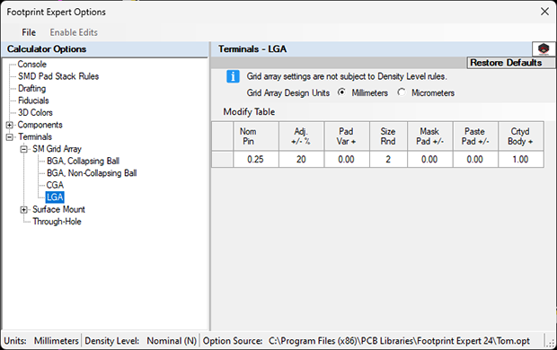
The Land Grid Array (LGA) is setup for you to insert the maximum column terminal
diameters and create the pad size adjustment, Pad Tolerance and Rounding,
Solder and Paste Mask sizes and Courtyard Excess value. The LGA terminal lead
is non-collapsing and requires a 20% increase in pad size.
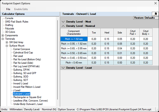
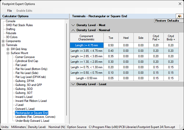
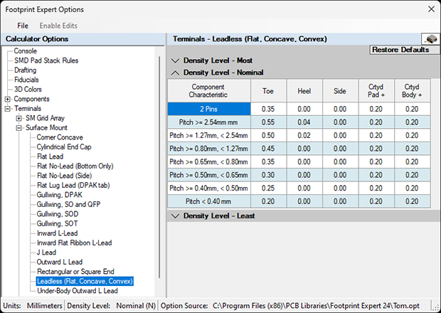
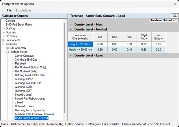
2. SURFACE MOUNT
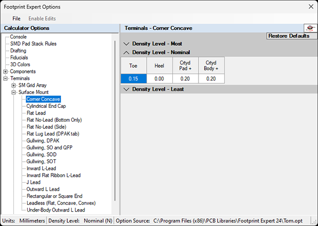
Corner Concave (Oscillator component family)
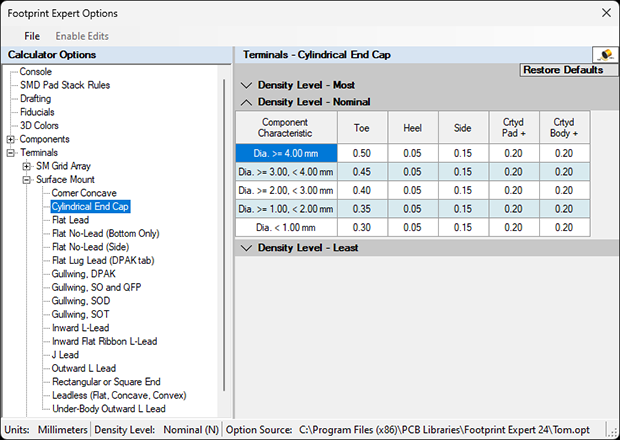
Cylindrical End Cap (MELF component families)
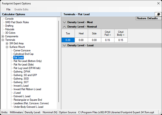
Flat Lead (SODFL & SOFL component families)
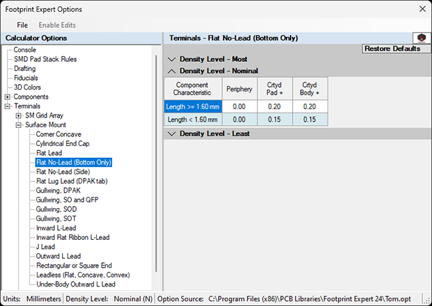
Flat Lead Bottom Only (Pullback Lead PSON & PQFN)
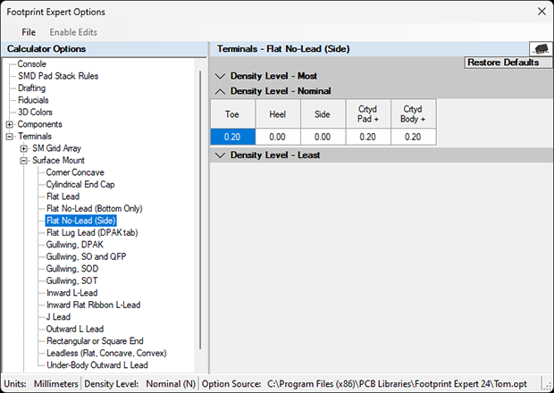
Flat Lead (Side) - (SON & QFN)
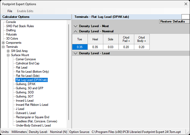
Flat Lug Lead (DPAK tab)
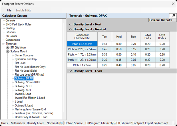
Gullwing, DPAK (for the DPAK package only)
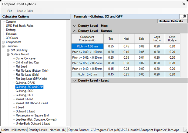
Gullwing, SO and QFP
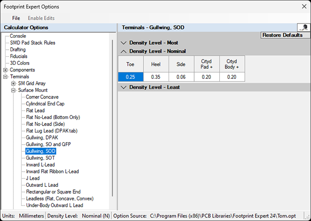
Gullwing, SOD
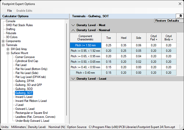
Gullwing, SOT
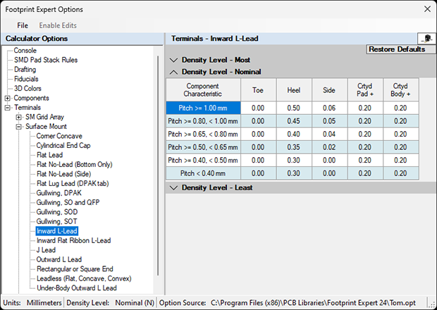
Inward L-Bend (SOL)
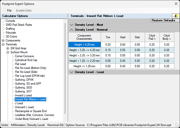
Inward Flat Ribbon L-Lead (Molded Body)
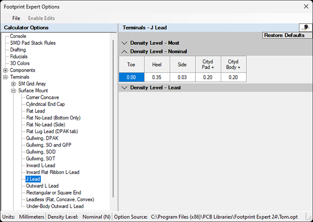
J-Lead
Outward L Lead
Rectangular or Square End (Chips)
Leadless (Flat, Concave, Convex) - Chip Arrays
Under-Body Outward L Lead (Capacitor, Aluminum Electrolytic CAPAE)
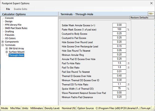
3. THROUGH-HOLE - these values are User Definable
- Solder Mask Annular Excess - (default is 1:1)
- Pask Mask (Pin-in-Paste technology) (default is 100%)
- Courtyard to Body Excess - (default 0.25)
- Courtyard to Pad Excess - (default 0.25)
- Hole Excess Over Round Lead (default 0.20)
- Hole Excess Over Rectangular Lead (default 0.15)
- Minimum Annular Ring - (default 0.20 for Class II fabrication)
- Pad-To-Hole Ratio - (default 1.5 or Hole Size X 1.5 = Pad Size)
- Pad-To-Slot Ratio - (default 1.8 or Slotted Hole Size X 1.8 - Pad Size)
- Pad Size Round to Nearest - default is 0.01
- Thermal ID Excess Over Hole - default is 0.40
- Minimum Thermal OD Excess Over ID - default is 0.30
- Thermal OD-To-Hole Ratio - default is 1.1
- Spoke Width (%of Thermal OD) - default is 75%
- Wave Placement Keepout Excess Over Pad - default is 0.00
- Minimum Pad-to-Pad Clearance - default is 0.20 (violating this rule with throw a warning)