

|
|
Standard Chip Package Case Codes & Dimensions |
Post Reply 
|
Page 12> |
| Author | |
Tom H 
Admin Group 

Joined: 05 Jan 2012 Location: San Diego, CA Status: Offline Points: 6074 |
 Post Options Post Options
") Thanks(0) Thanks(0)
 Quote Reply Quote Reply
 Topic: Standard Chip Package Case Codes & Dimensions Topic: Standard Chip Package Case Codes & DimensionsPosted: 07 Feb 2022 at 10:01am |
|
IPC-7351B contains the 3-Tier Density Levels for Land Patterns.
However, that document is 12 years old and out of date and it took information from the 1987 IPC-SM-782 which is obsolete. The solder Joint values are way too robust for today's technology. Footprint Expert solder joint goals are derived from IPC J-STD-001 standard as it's the main standard that all other standards are built upon. |
|
 |
|

|
|
|
|
|
AnonAnon
New User 
Joined: 07 Feb 2022 Status: Offline Points: 1 |
Post Options
Thanks(0)
Quote Reply
Posted: 07 Feb 2022 at 5:41am |
|
Hi Tom, Please excuse me if you've answered this a thousand times but I'm looking to find which standard defined the "Least" and "Most" limits for each footprint. I can see IPC-SM-782 defines the nominal and references equations in a section 3.3? I am happy to purchase the standard but wanted to ensure it contained the correct information before I purchase. Do the IPC standards only provide the nominal and one has to calculate the limits? Kind regards, David
|
|
|
|
|
Tom H
Admin Group
Joined: 05 Jan 2012 Location: San Diego, CA Status: Offline Points: 6074 |
Post Options
Thanks(0)
Quote Reply
Posted: 08 Sep 2021 at 8:32am |
|
Read the User Guide in the main installation folder under "Documents".
Select File > Save As > Your Master Options .opt |
|
|
|
|
phil.holden
Advanced User 
Joined: 14 Aug 2020 Status: Offline Points: 59 |
Post Options
Thanks(0)
Quote Reply
Posted: 08 Sep 2021 at 5:26am |
|
Hi Tom,
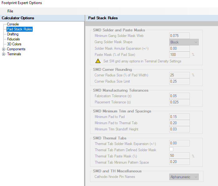
For my Enterprise Edition CLOUD Licensed the options under Pad Stack Rules are 'greyed' out. Does this mean that i am unable to control this globally?
 |
|
|
|
|
Tom H
Admin Group
Joined: 05 Jan 2012 Location: San Diego, CA Status: Offline Points: 6074 |
Post Options
Thanks(0)
Quote Reply
Posted: 07 Sep 2021 at 9:08am |
|
To get 3 or more passive packages to fit into the same Footprint, find parts with the same dimensions and tolerances. If the package dimensions are the same but the tolerances are different, then round the tolerances off so that they are all the same. Change this setting in "Tools > Options > Pad Stack Rules > SMD Corner Rounding > Corner Radius Limit".
|
|
|
|
|
phil.holden
Advanced User
Joined: 14 Aug 2020 Status: Offline Points: 59 |
Post Options
Thanks(0)
Quote Reply
Posted: 07 Sep 2021 at 4:08am |
|
As is common procedure, especially during these times with supply-chain issues. We try and specify x3 MPNs for all of our passive devices.
As there could be 3 substituted parts fitted all with differing terminal lengths. How am i best addressing this when creating a passive library? This is much less of a problem for active parts and connectors that are less 'interchangeable'. Thanks In addition to the above. I have noticed that the terminals sometimes overhang the pads when using 'rounded rectangle'. In your opinion, would this be a problem? 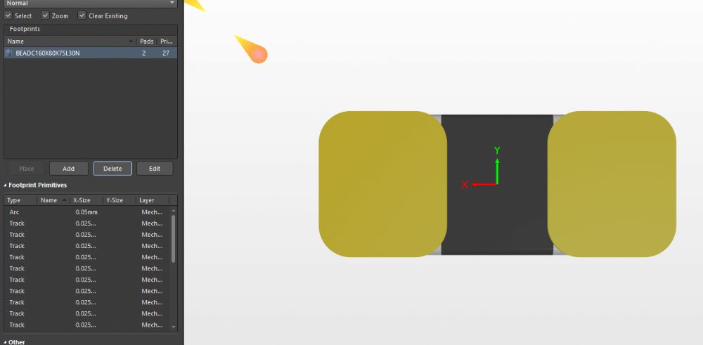 |
|
|
|
|
Tom H
Admin Group
Joined: 05 Jan 2012 Location: San Diego, CA Status: Offline Points: 6074 |
Post Options
Thanks(0)
Quote Reply
Posted: 02 Jul 2021 at 8:47am |
|
You need to attach a link to a PDF file zipped or a URL link to the datasheet would be better.
Then we can post the Proteus footprint. Are you using the Free V2021 Footprint Expert Pro for Proteus? You could create the footprint in a couple minutes. |
|
|
|
|
lladam
New User
Joined: 02 Jul 2021 Status: Offline Points: 1 |
Post Options
Thanks(0)
Quote Reply
Posted: 02 Jul 2021 at 6:26am |
|
Hi,
How to make a Proteus library part of MEGA2560 Pro Mini, or where can find one please. Because the board too small to put many pins on. Thanks
|
|
|
|
|
Tom H
Admin Group
Joined: 05 Jan 2012 Location: San Diego, CA Status: Offline Points: 6074 |
Post Options
Thanks(0)
Quote Reply
Posted: 25 Mar 2021 at 11:59am |
|
Use the mfr. recommended pattern for this new upcoming component family.
Some manufacturers use a periphery solder joint goal and other use a Toe, Heel and Side pad stack. This is a new Terminal Lead form that has not been fully tested by the world standards like IPC-J-STD-001 for solder joint acceptability. |
|
|
|
|
Arun7290
New User
Joined: 10 Mar 2021 Status: Offline Points: 7 |
Post Options
Thanks(0)
Quote Reply
Posted: 25 Mar 2021 at 11:52am |
|
Hi Tom,
Thanks for the reply. Can we use the above listed package sizes for Wraparound parts as well in the same case code? Because It is mentioned that the above case code dimensions are only for Standard Chips. And I am working on some wraparound packages of the standard case code. Can we use PCB library expert for footprint creation for these parts? Or Is it better to follow the Manufacturer recommended land pattern? 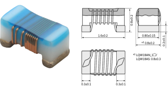 |
|
|
|
|
Post Reply
|
Page 12> |
| Tweet |
| Forum Jump | Forum Permissions You cannot post new topics in this forum You cannot reply to topics in this forum You cannot delete your posts in this forum You cannot edit your posts in this forum You cannot create polls in this forum You cannot vote in polls in this forum |


 Topic Options