

|
|
Rounded Rectangle Pad Shape |
Post Reply 
|
Page <12 |
| Author | |
Tom H 
Admin Group 

Joined: 05 Jan 2012 Location: San Diego, CA Status: Offline Points: 6074 |
 Post Options Post Options
") Thanks(0) Thanks(0)
 Quote Reply Quote Reply
 Posted: 18 Oct 2023 at 8:25am Posted: 18 Oct 2023 at 8:25am |
|
CAD vendors created Rounded Rectangle pad shape.
Most component datasheets recommend rectangular pad shape. IPC recommends oblong pad shape. Rounded Rectangle was primarily intended for the pad shape to be similar to the paste mask stencil aperture opening which is created by a laser and has rounded corner openings. 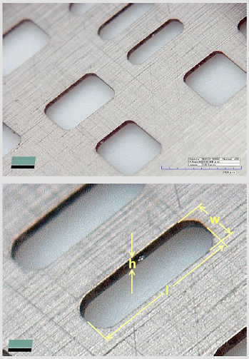 |
|
 |
|

|
|
|
|
|
eyoung
New User 
Joined: 18 Oct 2023 Status: Offline Points: 3 |
Post Options
Thanks(0)
Quote Reply
Posted: 18 Oct 2023 at 8:38am |
|
Our organization recently bought the IPC standard 7352 and it does consider rounded rectangle pads advantageous espically for Pb-free soldering processes(relevant to us) in comparison with rectangular pads I cant seem to find where it exactly states that rounded pads strengthens the solder joint, or where these values (below) were determined
Im trying to justify our organization to move towards an update to our procedures to use rounded rectangle pads so that we are up to industry standard. I want to be able to justify this change with a concrete IPC standard , if available. If so, could you point me to the exact one? Or maybe a study that demonstrates these claims. I appreciate your time and attention on this very much |
|
|
|
|
Tom H
Admin Group
Joined: 05 Jan 2012 Location: San Diego, CA Status: Offline Points: 6074 |
Post Options
Thanks(1)
Quote Reply
Posted: 18 Oct 2023 at 9:17am |
|
All IPC documents regarding PCB design and land patterns have been downgraded from "Standard" to "Guideline".
All new Texas Instruments datasheets provide a recommended solder pattern and the pad patterns have 0.05 mm corner radius. You decide what settings work best for you. The current Footprint Expert default for Maximum Radius is 0.20 mm (not 0.25 mm) but you can change the Maximum value to anything you want. You can also change all pad shapes to be Oblong or Rectangle. Or some component families can have oblong and some rectangle. You need to make your own choices, but I would discuss this with an assembly shop because the pad shape affects that manufacturing process. |
|
|
|
|
eyoung
New User
Joined: 18 Oct 2023 Status: Offline Points: 3 |
Post Options
Thanks(0)
Quote Reply
Posted: 07 Dec 2023 at 11:29am |
|
does PCB Footprint Expert - for Allegro include the new additions and recommendations that have been released in IPC-7352? Our company is considering a footprint/librarian program to help streamline our component creation process. |
|
|
|
|
Tom H
Admin Group
Joined: 05 Jan 2012 Location: San Diego, CA Status: Offline Points: 6074 |
Post Options
Thanks(0)
Quote Reply
Posted: 07 Dec 2023 at 11:36am |
|
V23 & the new V24 have IPC-7352 footprint naming convention and an Option file that turns off the Fabrication and Assembly tolerances and updates all negative solder joint goals to 0.00.
Note: All Option settings are user definable. |
|
|
|
|
Post Reply
|
Page <12 |
| Tweet |
| Forum Jump | Forum Permissions You cannot post new topics in this forum You cannot reply to topics in this forum You cannot delete your posts in this forum You cannot edit your posts in this forum You cannot create polls in this forum You cannot vote in polls in this forum |


 Topic Options