|
Footprint Expert
|
Source 1
|
Source 2
|

|

|

|
|
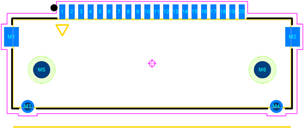
AUTO-GENERATED library parts use predefined or user-modified rules
– share across your organization;
RULES-based, auto-generated part library
|
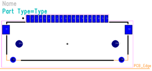
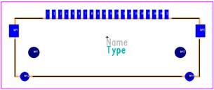
MANUALLY
CREATED by many different people, using countless rules – results in a board with
inconsistently built parts, far more prone to introduction of costly errors; massive
variations in parts inconducive to standardized rule-based library
|
|
Built to exact datasheet specification, either Metric or Mils
|
Units vary based on source, and Metric often
converted from Mils with rounded-off measurements; converting pin pitch often results in
leads not fully centered on pads
|
|
User-defined consistency of line widths for all parts
|
Many different line widths used across different footprints due to
lack of standard rules
|
|
Accurate contour courtyards are auto generated
|
Sloppy or non-existing contour
courtyards
|
|
Relevant data:
Footprint Name, Physical and Logical Descriptions, datasheet link, and more
|
Nothing, or inconsistent random data
|
|
Auto-generated keep outs on all non-plated holes for copper poly shapes,
traces and vias
|
Missing keep-out will cause DRC errors at the manufacturer if copper, traces,
and vias are placed within 0.25 mm of the non-plated hole
|
|
Pin 1 polarity markers for silkscreen and assembly
|
Pin 1 markings missing or vary in shape and in size
|
|
Footprint Origin at center of gravity
|
Footprint Origins randomly placed
|
|
Uniform, silkscreen outlines are whole objects mapped to the maximum package dimensions
|
Silkscreen is fragmented and mapped to the nominal package
dimensions
|
|
Clear, consistent, intelligently placed markings to minimizes
use of board space
|
Inconsistent
and extra markings and excessive courtyards requires more placement space
|
|
Consistent silkscreen trimming around all pads
|
Inconsistent and random silkscreen
trimming around pads
|
|
Solder Mask swell auto-applied and configurable
|
Inconsistent solder mask swell from one footprint to another
|
|
Through-hole pad stack hole sizes automatically
defined by maximum terminal lead diameter, and pad size auto-calculated
by 1.5 x hole diameter
|
Lack of published, consistent rules to define through-hole
pad stacks make it impossible for proper quality control of resulting
footprint, results in
capriciously calculated footprints
|
|
Non-plated holes have smaller pad sizes to prevent
copper slivers after drilling process
|
Non-plated
holes have a pad size equal to the hole size create risk of copper slivers after the drilling process; the plane antipad is randomly defined with
no obvious rules
|


 Post Options
 Thanks(0)
 Quote
Quote  Reply
Reply
 Topic: What's Wrong with Your Footprint?!


