
 |

|
IPC-J-STD-001 Chip Component Solder Joints |
Post Reply 
|
| Author | |
Tom H 
Admin Group 

Joined: 05 Jan 2012 Location: San Diego, CA Status: Offline Points: 5718 |
 Post Options Post Options
 Thanks(2) Thanks(2)
 Quote Quote  Reply Reply
 Topic: IPC-J-STD-001 Chip Component Solder Joints Topic: IPC-J-STD-001 Chip Component Solder JointsPosted: 27 Dec 2019 at 12:11pm |
|
The Chip Package is the most widely used in the electronics
industry. Chip components have an average of 80% of the total parts on a
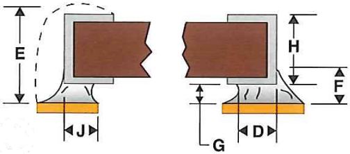
typical PCB assembly. Here is an image of the average chip terminal lead form.
Let’s compare the differences between IPC-J-STD-001 and
IPC-7351B standards. IPC-J-STD-001 uses 3 classes to define solder joint goal
acceptability for various electronic products. CLASS 1 –
General Electronic Products Includes products suitable for applications where the major
requirement is function of the completed assembly. Toys CLASS 2 –
Dedicated Service Electronic Products Includes products where continued performance and extended
life is required, and for which uninterrupted service is desired but not
critical. Typically, the end-use environment would not cause failures.
Computers & Phones CLASS 3 –
High Performance Electronic Products Includes products where continued high performance or
performance-on-demand is critical, equipment downtime cannot be tolerated,
end-use environment may be uncommonly harsh, and the equipment must function
when required, such as life support or other critical systems. Military &
Medical IPC-J-STD-001 defines the requirements for electronic
assemblies. Land pattern footprint pad sizes and locations play a significant
role in meeting these requirements. The IPC-7351 guideline falls under
J-STD-001 to define the solder joint goals for Toe, Heel and Side values and
the land pattern and pad stack naming conventions. The footprint pad size is determined by the terminal lead
size, the terminal lead tolerances, the manufacturing tolerances for
fabrication and assembly and the Toe, Heel and Side solder joint goals as
defined in the IPC-7351 guideline. The Toe solder joint goal is the most important for the Chip
Terminal Lead and the J-STD-001 Minimum Fillet Height for a Chip Component for
the Toe Goal is: The F
dimension for Toe Fillet for Class 1 & Class 2 Fabrication is:
The F
dimension for Toe Fillet for Class 3 Fabrication is:
Example: For Class 3, let’s say that the 0805 Chip Capacitor
is 4.00 mm height. 25% of 4 = 1.00 mm. But the IPC-J-STD-001 standard says the
0.50 mm is an acceptable solder fillet height because it’s less than 1.00 mm.
But what about an 01005 chip resistor with a 0.13 mm height? Using a 0.075
stencil thickness, J-STD-001 recommends a Toe fillet of (G) 0.07 + 25% (H) 0.03
mm = 0.10 mm. But (G) is actually less than 0.05 mm after reflow.  If the Toe pad length is too long, there will be excessive solder. When going into a reflow oven, if there is excessive solder and pin 1 hits the heat first, the excessive solder will melt and pull the chip up into a tombstone position. To eliminate tombstoning, the pad Toe must not exceed the J-STD-001 requirements.
Here are the IPC-7351B tables for all chip packages including Resistors, Capacitors, Diodes, Inductors, Antennas, Ferrite Beads, Filters, Fuses, LED’s, Thermistors and Varistors for 3 density levels, Most, Nominal and Least pad size.
Note that for all chips longer than a 0603, the Nominal Toe
value is 0.35 mm for 0603, 0805, 1206, 1210, 1812, 2010 and 2512, regardless of
their height. And for every chip package less than 0603 the Nominal Toe value
is 0.20 for 03015, 01005, 0201 and 0402. Also note that the difference between
density levels for chips larger than 0603 is +/- 0.20 mm for Most and Least density
levels and chips smaller than 0603 have a +/- 0.10 mm difference between Most
and Least density levels. PCB Libraries, Inc. has a philosophy that every chip size
should have a unique Toe value that is aligned with J-STD-001 mathematical
model for the acceptable solder joint. Here is a table for the default values in Library Expert,
but all of these settings are user definable to best meet your assembly
attachment requirements. Also note that there is a +/- 0.10 mm between Most and
Least density levels for all chips.  PCB Libraries, Inc. refers to this concept as “Incremental
Pad Stacks” for the sole purpose of achieving the best solder joint goals in
the assembly process. You can download the entire Library Expert Solder Joint
Goals Excel spreadsheet here – www.pcblibraries.com/downloads
or if you’re using Library Expert, the Excel spreadsheet is on your computer in
this folder - C:\Program Files (x86)\PCB Libraries\Library Expert
2019\Documents\Library Expert Solder Joint Goal Tables.xlsx Note that there are negative values for some Heel and Side
solder joints. This is to compensate for the Fabrication and Assembly Tolerances
(approximately 0.04 to 0.05 mm) in the IPC-7351 mathematical model. The
Fabrication and Assembly Tolerances have been part of the IPC mathematical
model since 1987. In the past 33 years, the fabrication and assembly processes
have been improved so much that these tolerances are no longer applicable to
todays advanced machines. Also, most fabrication shops swell the outer layers
to compensate for their etching process. Adding an additional fabrication tolerance
to the pad size calculation is a “Double (duplicate) Tolerance” and is unnecessary.
We recommended that the Fabrication and Assembly Tolerances
be turned off to 0.00 and all negative solder joint goals also be turned to
0.00. This would give the user much better control of the pad stack calculation.
But this is an individual choice that every company must make on their own. We
hope that the unreleased IPC-7351C will make this adjustment to the
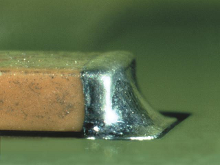
mathematical model. It’s also important to note that Lead Solder flows much
better than Lead-Free Solder. Here is an image of a chip with lead solder. You
can visually see that the solder flows from the pad Toe up the side of the chip
terminal. Also note that the pad Heel is 0.00 and flush with the chip terminal.
 Here is an image of chips using Lead-Free solder. Most of
the solder just stays on the pad and does not flow up the side of the chip terminal
lead like Lead Solder. Also, this example illustrates excessive pad Toe. This consumes
important PCB real estate, wastes solder and does nothing to add to the solder
joint quality. |
|
 |
|
 |
|
stanleycayochok 
Active User 
Joined: 04 Apr 2016 Status: Offline Points: 23 |
 Post Options Post Options
 Thanks(0) Thanks(0)
 Quote Quote  Reply Reply
 Posted: 26 Jan 2021 at 11:26pm Posted: 26 Jan 2021 at 11:26pm |
|
Hi Tom,
Does these rules apply to inverted chip package size like 0204, 0306, 0508, etc where in the the terminal is on the longer side?
|
|
 |
|
Tom H 
Admin Group 

Joined: 05 Jan 2012 Location: San Diego, CA Status: Offline Points: 5718 |
 Post Options Post Options
 Thanks(0) Thanks(0)
 Quote Quote  Reply Reply
 Posted: 27 Jan 2021 at 9:42am Posted: 27 Jan 2021 at 9:42am |
|
Yes, keep the inverted parts in the same category as the standard parts.
i.e.: 0805 & 0508 are the same solder joint goals. |
|
 |
|
stanleycayochok 
Active User 
Joined: 04 Apr 2016 Status: Offline Points: 23 |
 Post Options Post Options
 Thanks(0) Thanks(0)
 Quote Quote  Reply Reply
 Posted: 26 Feb 2021 at 1:12am Posted: 26 Feb 2021 at 1:12am |
|
Thanks Tom!
|
|
 |
|
matt_hageman 
New User 
Joined: 06 Jan 2022 Status: Offline Points: 1 |
 Post Options Post Options
 Thanks(0) Thanks(0)
 Quote Quote  Reply Reply
 Posted: 06 Jan 2022 at 9:47pm Posted: 06 Jan 2022 at 9:47pm |
|
Hi Tom,
I've been noodling around for least density footprints and I enjoyed this post thoroughly, thank you! Even though the fate of IPC-7351C seems questionable, I see that in a slide deck you created that 0603's and higher got 0.12mm courtyard excess and 0402's had 0.15mm. Is that true anymore? I see 0.10mm courtyard excess in the goal tables and I'd like to roll with it, but wanted to understand if that was discouraged Best, -Matt
|
|
 |
|
Tom H 
Admin Group 

Joined: 05 Jan 2012 Location: San Diego, CA Status: Offline Points: 5718 |
 Post Options Post Options
 Thanks(0) Thanks(0)
 Quote Quote  Reply Reply
 Posted: 07 Jan 2022 at 9:21am Posted: 07 Jan 2022 at 9:21am |
|
Matt, there is an Option setting in Tools > Options > Drafting > Courtyard Outlines > Expand Courtyard to Include Silkscreen. This will push the Courtyard out so that the Silkscreen Outline is inside the Courtyard Outline.
Download and install the V2022.01 pre-release and create an 0402 and you'll see new silkscreen outlines for small chips. |
|
 |
|
Post Reply 
|
|
| Tweet |
| Forum Jump | Forum Permissions  You cannot post new topics in this forum You cannot reply to topics in this forum You cannot delete your posts in this forum You cannot edit your posts in this forum You cannot create polls in this forum You cannot vote in polls in this forum |