
 |

|
Explain Custom Padname |
Post Reply 
|
| Author | |
PLTcbv 
Advanced User 
Joined: 21 Aug 2012 Location: the Netherlands Status: Offline Points: 134 |
 Post Options Post Options
 Thanks(0) Thanks(0)
 Quote Quote  Reply Reply
 Topic: Explain Custom Padname Topic: Explain Custom PadnamePosted: 21 Aug 2013 at 2:04am |
|
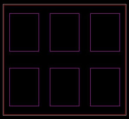
If I create a TAB padstack for a TO, DPAK shape in PCB LE Lite and built a padstack with Expedition ASCII output I get "r612_555m622_565p6xr147_192"
 The paste mask name is 6xr147_192. This is a custom pad in Expedition with the name "COMPLEX 5.552X4.7 A26.0944 S6".
Please explain the custom pad syntax.
|
|
 |
|

|
|
 |
|
Tom H 
Admin Group 

Joined: 05 Jan 2012 Location: San Diego, CA Status: Offline Points: 6033 |
 Post Options Post Options
 Thanks(0) Thanks(0)
 Quote Quote  Reply Reply
 Posted: 21 Aug 2013 at 6:42am Posted: 21 Aug 2013 at 6:42am |
|
r612_555m622_565p6xr147_192
r = rectangle 612_555 = length_width of pad m = solder mask 622_565 = length_width of solder mask p = paste mask 6x = 6 paste mask objects r = rectangle 147_196 = size of each paste mask rectangle You need to download the IPC-7351 padstack naming convention here - Padstacks |
|
 |
|
PLTcbv 
Advanced User 
Joined: 21 Aug 2012 Location: the Netherlands Status: Offline Points: 134 |
 Post Options Post Options
 Thanks(0) Thanks(0)
 Quote Quote  Reply Reply
 Posted: 21 Aug 2013 at 6:53am Posted: 21 Aug 2013 at 6:53am |
|
Tom, I think you misunderstood me.
The explanation is for the generated custom pad with the name COMPLEX 5.552X4.7 A26.0944 S6. Can you explain this syntax? |
|
 |
|
Tom H 
Admin Group 

Joined: 05 Jan 2012 Location: San Diego, CA Status: Offline Points: 6033 |
 Post Options Post Options
 Thanks(0) Thanks(0)
 Quote Quote  Reply Reply
 Posted: 03 Sep 2013 at 2:31pm Posted: 03 Sep 2013 at 2:31pm |
|
No, where did that come from?
|
|
 |
|
PLTcbv 
Advanced User 
Joined: 21 Aug 2012 Location: the Netherlands Status: Offline Points: 134 |
 Post Options Post Options
 Thanks(0) Thanks(0)
 Quote Quote  Reply Reply
 Posted: 03 Sep 2013 at 11:22pm Posted: 03 Sep 2013 at 11:22pm |
|
This is the custom pad shape name in Expedition when used with ASCII input from LE Lite.
Maybe Chris can answer this question.
|
|
 |
|
chrisa_pcb 
Moderator Group 
Joined: 29 Jul 2012 Location: San Diego Status: Offline Points: 772 |
 Post Options Post Options
 Thanks(0) Thanks(0)
 Quote Quote  Reply Reply
 Posted: 04 Sep 2013 at 9:51am Posted: 04 Sep 2013 at 9:51am |
Length X Width with an area of 26.0944, 6 squares. Its simply a way of differentiating that complex padstack from others. |
|
 |
|
PLTcbv 
Advanced User 
Joined: 21 Aug 2012 Location: the Netherlands Status: Offline Points: 134 |
 Post Options Post Options
 Thanks(0) Thanks(0)
 Quote Quote  Reply Reply
 Posted: 04 Sep 2013 at 11:10pm Posted: 04 Sep 2013 at 11:10pm |
|
Thanks Chris.
The Length, Width and 6 squares where clear. Only the A26.0944 was puzzling me. Now it is clear.
|
|
 |
|
Post Reply 
|
|
| Tweet |
| Forum Jump | Forum Permissions  You cannot post new topics in this forum You cannot reply to topics in this forum You cannot delete your posts in this forum You cannot edit your posts in this forum You cannot create polls in this forum You cannot vote in polls in this forum |