Explain Custom Padname
Printed From: PCB Libraries Forum
Category: PCB Footprint Expert
Forum Name: Questions & Answers
Forum Description: issues and technical support
URL: https://www.PCBLibraries.com/forum/forum_posts.asp?TID=1087
Printed Date: 22 Mar 2026 at 8:13pm
Topic: Explain Custom Padname
Posted By: PLTcbv
Subject: Explain Custom Padname
Date Posted: 21 Aug 2013 at 2:04am
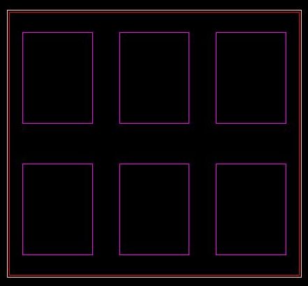
If I create a TAB padstack for a TO, DPAK shape in PCB LE Lite and built a padstack with Expedition ASCII output I get "r612_555m622_565p6xr147_192"
 The paste mask name is 6xr147_192. This is a custom pad in Expedition with the name "COMPLEX 5.552X4.7 A26.0944 S6".
Please explain the custom pad syntax.
|
Replies:
Posted By: Tom H
Date Posted: 21 Aug 2013 at 6:42am
|
r612_555m622_565p6xr147_192 r = rectangle 612_555 = length_width of pad m = solder mask 622_565 = length_width of solder mask p = paste mask 6x = 6 paste mask objects r = rectangle 147_196 = size of each paste mask rectangle You need to download the IPC-7351 padstack naming convention here - http://www.pcblibraries.com/forum/ipc7x51-padstack-naming-convention-metric-units_topic36.html" rel="nofollow - Padstacks ------------- Stay connected - follow us! https://twitter.com/PCBLibraries" rel="nofollow - X - http://www.linkedin.com/company/pcb-libraries-inc-/" rel="nofollow - LinkedIn |
Posted By: PLTcbv
Date Posted: 21 Aug 2013 at 6:53am
|
Tom, I think you misunderstood me. The explanation is for the generated custom pad with the name COMPLEX 5.552X4.7 A26.0944 S6. Can you explain this syntax? |
Posted By: Tom H
Date Posted: 03 Sep 2013 at 2:31pm
|
No, where did that come from?
------------- Stay connected - follow us! https://twitter.com/PCBLibraries" rel="nofollow - X - http://www.linkedin.com/company/pcb-libraries-inc-/" rel="nofollow - LinkedIn |
Posted By: PLTcbv
Date Posted: 03 Sep 2013 at 11:22pm
|
This is the custom pad shape name in Expedition when used with ASCII input from LE Lite. Maybe Chris can answer this question.
|
Posted By: chrisa_pcb
Date Posted: 04 Sep 2013 at 9:51am
Length X Width with an area of 26.0944, 6 squares. Its simply a way of differentiating that complex padstack from others. |
Posted By: PLTcbv
Date Posted: 04 Sep 2013 at 11:10pm
|
Thanks Chris. The Length, Width and 6 squares where clear. Only the A26.0944 was puzzling me. Now it is clear.
|
 PLTcbv wrote: