|
|
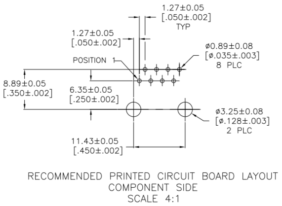
RJ45 footprint |
Post Reply 
|
| Author | |
loic-7 
New User 
Joined: 27 Dec 2013 Status: Offline Points: 3 |
 Post Options Post Options
") Thanks(0) Thanks(0)
 Quote Reply Quote Reply
 Topic: RJ45 footprint Topic: RJ45 footprintPosted: 06 Jan 2014 at 7:47am |
|
Hello everyone,
I need to find the footprints of a RJ45 connector. It's a te connectivity connector. Here, you can find the reference : http://www.te.com/catalog/pn/en/5520259-4. I'm a beginner in Allegro PCB Designer, so I will take all of your advices. Thanks.
|
|
 |
|
|
|
|
Nick B
Admin Group 
Joined: 02 Jan 2012 Status: Offline Points: 1904 |
Post Options
Thanks(1)
Quote Reply
Posted: 06 Jan 2014 at 9:55am |
|
The Library Expert can build this using the Footprint Designer module. |
|
|
|
|
Tom H
Admin Group

Joined: 05 Jan 2012 Location: San Diego, CA Status: Offline Points: 5716 |
Post Options
Thanks(1)
Quote Reply
Posted: 06 Jan 2014 at 12:55pm |
|
Using "Footprint Designer", you can easily create this phone jack using 2 pad stacks. The Parts on Demand (POD) website will soon be on-line starting with over 225,000 Part Numbers and we're adding new parts as fast as we can. This TE Connectivity Footprint only needs to be created once by someone and then upload the FPX file to POD to share it with the entire electronics industry. One person has to build it right and no one will ever have to build it again. Library Expert currently supports 20 different CAD tool interfaces.
|
|
|
|
|
loic-7
New User
Joined: 27 Dec 2013 Status: Offline Points: 3 |
Post Options
Thanks(0)
Quote Reply
Posted: 07 Jan 2014 at 9:22am |
|
Hello, thank you for your answers. I followed the tutorial "How to design a RJ45 connector", it allowed me to design the connector's footprint and save it in a new library. The library's extension is .fpx. How can I import this library in Orcad ? The extension in Orcad for the footprints are .psm and .dra, how can I attach my new footprint to my component in my schematic. Thanks for your replies. |
|
|
|
|
Nick B
Admin Group
Joined: 02 Jan 2012 Status: Offline Points: 1904 |
Post Options
Thanks(0)
Quote Reply
Posted: 07 Jan 2014 at 9:34am |
|
|
|
Post Reply
|
|
| Tweet |
| Forum Jump | Forum Permissions You cannot post new topics in this forum You cannot reply to topics in this forum You cannot delete your posts in this forum You cannot edit your posts in this forum You cannot create polls in this forum You cannot vote in polls in this forum |


 Topic Options