

|
|
Non-Standard Land Patterns |
Post Reply 
|
| Author | |
m.elsayed 
Expert User 
Joined: 22 Sep 2016 Status: Offline Points: 212 |
 Post Options Post Options
") Thanks(0) Thanks(0)
 Quote Reply Quote Reply
 Topic: Non-Standard Land Patterns Topic: Non-Standard Land PatternsPosted: 9 hours 48 minutes ago at 5:46am |
|
How to apply the below statement in Footprint Expert? Create a Non-standard component package Land Pattern by calculating the minimum Toe and Heel requirements from the lead dimension given in the datasheet considering all the DFx standards in case the component manufacturer does not provide a Recommended Land Pattern in the product datasheet/drawing. |
|
 |
|

|
|
|
|
|
Tom H
Admin Group 

Joined: 05 Jan 2012 Location: San Diego, CA Status: Offline Points: 5943 |
Post Options
Thanks(0)
Quote Reply
Posted: 6 hours 44 minutes ago at 8:50am |
|
I've never seen a non-standard component package where the manufacturer does not provide a recommended Land Pattern.
However, if the case ever occurred where you need to calculate a pattern, you need to know the terminal lead style. 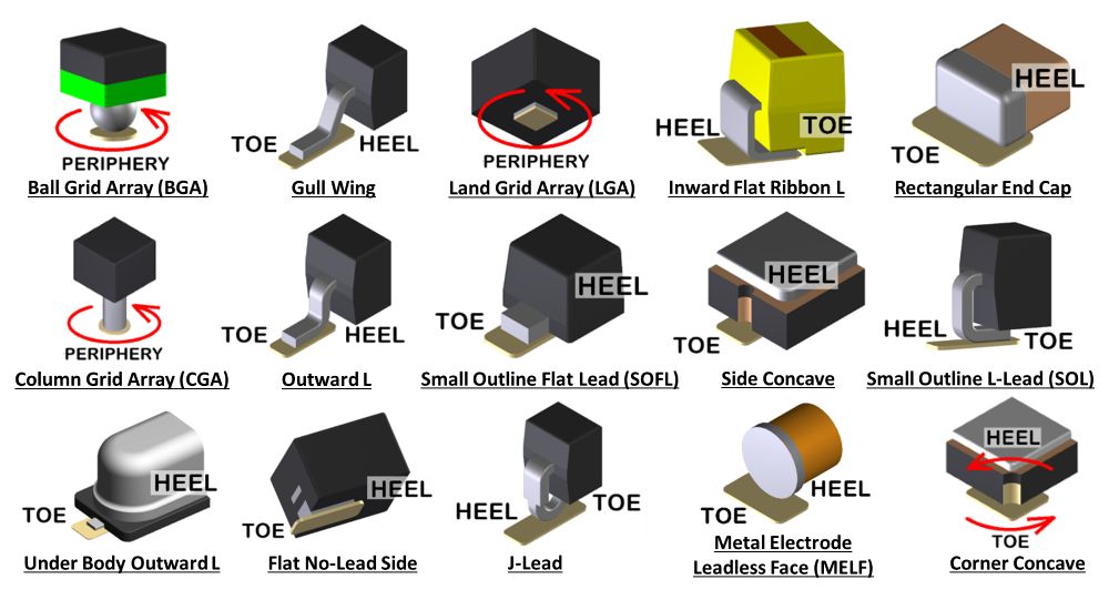 You can open a component family calculator that uses one of the terminal lead styles and enter package and terminal dimensions. Then move the footprint to FP Designer to customized the pad stack pattern. We normally start the creation of a non-standard footprint in a component family calculator and adjust the pad shape and solder mask swell prior to moving the footprint to FP Designer. |
|
|
|
|
Post Reply
|
|
| Tweet |
| Forum Jump | Forum Permissions You cannot post new topics in this forum You cannot reply to topics in this forum You cannot delete your posts in this forum You cannot edit your posts in this forum You cannot create polls in this forum You cannot vote in polls in this forum |


 Topic Options