Non-Standard Land Patterns
Printed From: PCB Libraries Forum
Category: PCB Footprint Expert
Forum Name: Questions & Answers
Forum Description: issues and technical support
URL: https://www.PCBLibraries.com/forum/forum_posts.asp?TID=3571
Printed Date: 24 Jul 2026 at 1:16pm
Topic: Non-Standard Land Patterns
Posted By: m.elsayed
Subject: Non-Standard Land Patterns
Date Posted: 29 Oct 2025 at 5:46am
|
How to apply the below statement in Footprint Expert? Create a Non-standard component package Land Pattern by calculating the minimum Toe and Heel requirements from the lead dimension given in the datasheet considering all the DFx standards in case the component manufacturer does not provide a Recommended Land Pattern in the product datasheet/drawing. |
Replies:
Posted By: Tom H
Date Posted: 29 Oct 2025 at 8:50am
|
I've never seen a non-standard component package where the manufacturer does not provide a recommended Land Pattern. However, if the case ever occurred where you need to calculate a pattern, you need to know the terminal lead style. 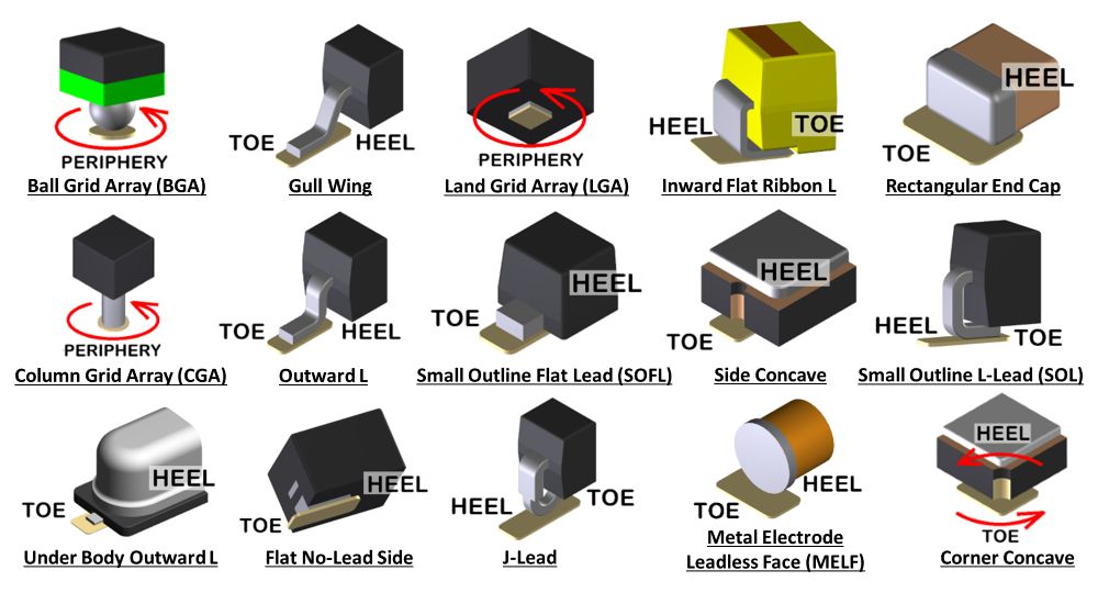 You can open a component family calculator that uses one of the terminal lead styles and enter package and terminal dimensions. Then move the footprint to FP Designer to customized the pad stack pattern. We normally start the creation of a non-standard footprint in a component family calculator and adjust the pad shape and solder mask swell prior to moving the footprint to FP Designer. ------------- Stay connected - follow us! https://twitter.com/PCBLibraries" rel="nofollow - X - http://www.linkedin.com/company/pcb-libraries-inc-/" rel="nofollow - LinkedIn |