

|
|
Leaded Horizontal TO-220 Pad Association |
Post Reply 
|
| Author | |
caclark 
Advanced User 
Joined: 24 Oct 2012 Location: Cincinnati, OH Status: Offline Points: 177 |
 Post Options Post Options
") Thanks(0) Thanks(0)
 Quote Reply Quote Reply
 Topic: Leaded Horizontal TO-220 Pad Association Topic: Leaded Horizontal TO-220 Pad AssociationPosted: 20 Mar 2013 at 11:46am |
|
I am currently trying to build a TO-220 leaded transistor in PCB Libraries. All goes fine with the creation within the tool graphically, but when I import it into my PADS library (ver 9.3.1 if relevant) the 4 th pin does not have the large thermal pad associated to the hole (see image).
I also noticed that graphically the large pad shows as expected (see image). And as for the version I am on 2012.47 In any case I will add them directly to this post anyway. 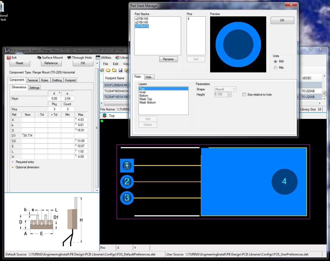 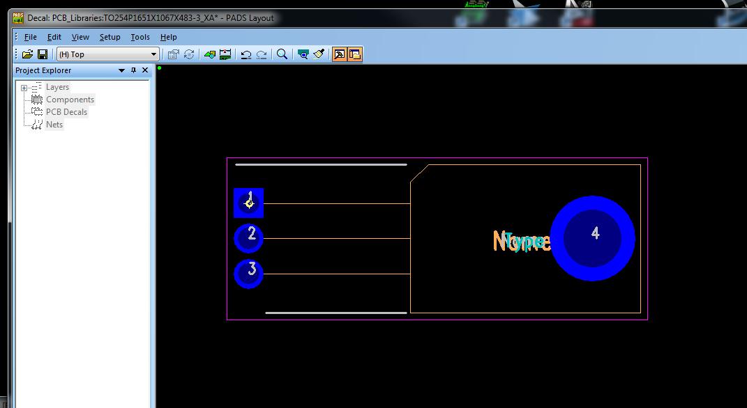 |
|
 |
|
|
|
|
rdl86626
Advanced User

Joined: 20 Jul 2012 Location: Hollister, CA Status: Offline Points: 83 |
Post Options
Thanks(0)
Quote Reply
Posted: 08 May 2013 at 12:17pm |
|
I was also building a TO-220FP footprint, horizontal. I put the numbers in, saved it to my library, clicked on it again and it turns vertical with all the wrong dimensions, h was 16.4 now says it is 3.6. I output it to OrCAD PCB Editor and it comes out ok. Also I don't understand what the b dimension is. Is it the thickness of the terminal? I am using 0.51 version. A little confused.
Rick
|
|
|
|
|
Post Reply
|
|
| Tweet |
| Forum Jump | Forum Permissions You cannot post new topics in this forum You cannot reply to topics in this forum You cannot delete your posts in this forum You cannot edit your posts in this forum You cannot create polls in this forum You cannot vote in polls in this forum |


 Topic Options