Leaded Horizontal TO-220 Pad Association
Printed From: PCB Libraries Forum
Category: PCB Footprint Expert
Forum Name: Questions & Answers
Forum Description: issues and technical support
URL: https://www.PCBLibraries.com/forum/forum_posts.asp?TID=892
Printed Date: 25 Jul 2026 at 6:18am
Topic: Leaded Horizontal TO-220 Pad Association
Posted By: caclark
Subject: Leaded Horizontal TO-220 Pad Association
Date Posted: 20 Mar 2013 at 11:46am
|
I am currently trying to build a TO-220 leaded transistor in PCB Libraries. All goes fine with the creation within the tool graphically, but when I import it into my PADS library (ver 9.3.1 if relevant) the 4 th pin does not have the large thermal pad associated to the hole (see image). I also noticed that graphically the large pad shows as expected (see image). And as for the version I am on 2012.47 In any case I will add them directly to this post anyway. 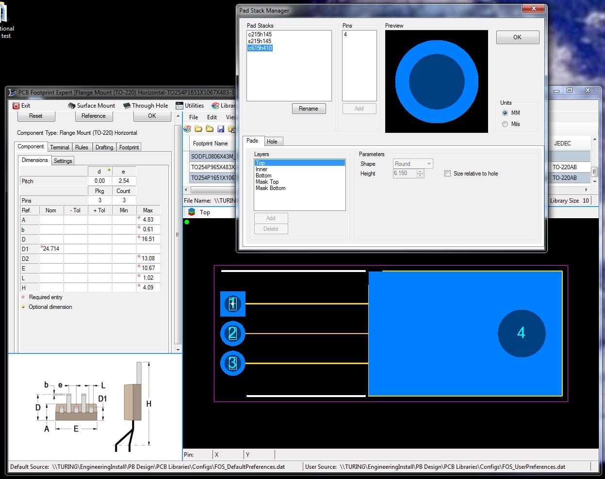 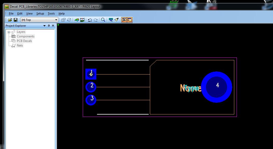 |
Replies:
Posted By: rdl86626
Date Posted: 08 May 2013 at 12:17pm
|
I was also building a TO-220FP footprint, horizontal. I put the numbers in, saved it to my library, clicked on it again and it turns vertical with all the wrong dimensions, h was 16.4 now says it is 3.6. I output it to OrCAD PCB Editor and it comes out ok. Also I don't understand what the b dimension is. Is it the thickness of the terminal? I am using 0.51 version. A little confused.
Rick
|