

|
|
No Silkscreen Created For QFN |
Post Reply 
|
| Author | |
chads108 
Active User 

Joined: 17 Oct 2012 Location: Plano, TX Status: Offline Points: 35 |
 Post Options Post Options
") Thanks(0) Thanks(0)
 Quote Reply Quote Reply
 Topic: No Silkscreen Created For QFN Topic: No Silkscreen Created For QFNPosted: 28 Nov 2012 at 8:36am |
|
I have a QFN package I created with Library Expert, but the silkscreen did not get defined.
Link to part in question: http://www.enpirion.com/products-dcdc-converter-step-down-buck-ep53f8qi.htm Chad |
|
 |
|

|
|
|
|
|
Tom H
Admin Group 

Joined: 05 Jan 2012 Location: San Diego, CA Status: Offline Points: 6088 |
Post Options
Thanks(0)
Quote Reply
Posted: 28 Nov 2012 at 8:46am |
|
The component leads are very close to the package corners where the silkscreen is normally placed outside the component package and inside the placement courtyard.
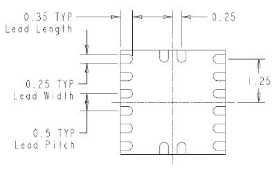 You need to manually add a line or dot polarity mark in your CAD tool editor. This is a workaround until we add interactive editing in the PCB Footprint Editor. |
|
|
|
|
chads108
Active User
Joined: 17 Oct 2012 Location: Plano, TX Status: Offline Points: 35 |
Post Options
Thanks(0)
Quote Reply
Posted: 28 Nov 2012 at 8:49am |
|
So you would recommend leaving all silkscreen off of this part other than the polarity mark?
|
|
|
|
|
Tom H
Admin Group
Joined: 05 Jan 2012 Location: San Diego, CA Status: Offline Points: 6088 |
Post Options
Thanks(0)
Quote Reply
Posted: 28 Nov 2012 at 9:08am |
|
Using the CAD tool editor I would make my part look like this -
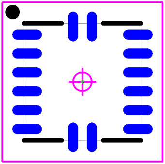 The current PCB Footprint Editor is a basic "Template" tool for "Standard Component Packages". This QFN is just outside the "Standard" category. So until the FPE program introduces interactive editing you'll have to spend a couple minutes adding some custom silkscreen lines using your CAD tool library editor. |
|
|
|
|
Post Reply
|
|
| Tweet |
| Forum Jump | Forum Permissions You cannot post new topics in this forum You cannot reply to topics in this forum You cannot delete your posts in this forum You cannot edit your posts in this forum You cannot create polls in this forum You cannot vote in polls in this forum |


 Topic Options