No Silkscreen Created For QFN
Printed From: PCB Libraries Forum
Category: PCB Footprint Expert
Forum Name: Questions & Answers
Forum Description: issues and technical support
URL: https://www.PCBLibraries.com/forum/forum_posts.asp?TID=704
Printed Date: 24 Jul 2026 at 9:08pm
Topic: No Silkscreen Created For QFN
Posted By: chads108
Subject: No Silkscreen Created For QFN
Date Posted: 28 Nov 2012 at 8:36am
|
I have a QFN package I created with Library Expert, but the silkscreen did not get defined. Link to part in question: http://www.enpirion.com/products-dcdc-converter-step-down-buck-ep53f8qi.htm" rel="nofollow - http://www.enpirion.com/products-dcdc-converter-step-down-buck-ep53f8qi.htm Chad |
Replies:
Posted By: Tom H
Date Posted: 28 Nov 2012 at 8:46am
The component leads are very close to the package corners where the silkscreen is normally placed outside the component package and inside the placement courtyard. 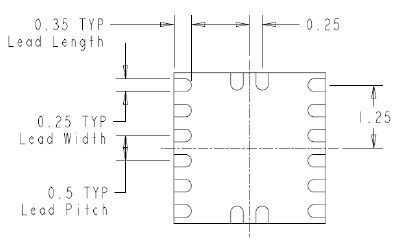 You need to manually add a line or dot polarity mark in your CAD tool editor. This is a workaround until we add interactive editing in the PCB Footprint Editor. |
Posted By: chads108
Date Posted: 28 Nov 2012 at 8:49am
| So you would recommend leaving all silkscreen off of this part other than the polarity mark? |
Posted By: Tom H
Date Posted: 28 Nov 2012 at 9:08am
Using the CAD tool editor I would make my part look like this -  The current PCB Footprint Editor is a basic "Template" tool for "Standard Component Packages". This QFN is just outside the "Standard" category. So until the FPE program introduces interactive editing you'll have to spend a couple minutes adding some custom silkscreen lines using your CAD tool library editor. |