|
|
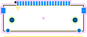
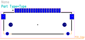
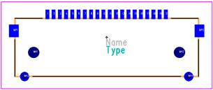
What's Wrong with Your Footprint?! |
Post Reply 
|
| Author | ||||||||||||||||||||||||||||||||||||||||||||||||
Nick B 
Admin Group 

Joined: 02 Jan 2012 Status: Offline Points: 2016 |
 Post Options Post Options
") Thanks(0) Thanks(0)
 Quote Reply Quote Reply
 Topic: What's Wrong with Your Footprint?! Topic: What's Wrong with Your Footprint?!Posted: 31 Jul 2024 at 3:57am |
|||||||||||||||||||||||||||||||||||||||||||||||
 The
Footprint Expert automates footprints to perfection. Professional,
detailed, and accurate parts – all built consistently with identical rules,
regardless of how many people are involved in your library development. Get your FREE Footprint Calculator or Footprint Expert Evaluation License: https://www.PCBLibraries.com/Register Call us - 847-557-2300 |
||||||||||||||||||||||||||||||||||||||||||||||||
 |
||||||||||||||||||||||||||||||||||||||||||||||||

|
||||||||||||||||||||||||||||||||||||||||||||||||
|
||||||||||||||||||||||||||||||||||||||||||||||||
|
Nick B
Admin Group
Joined: 02 Jan 2012 Status: Offline Points: 2016 |
Post Options
Thanks(0)
Quote Reply
Posted: 30 Jan 2025 at 12:13pm |
|||||||||||||||||||||||||||||||||||||||||||||||
|
The free Footprint Calculator and the Footprint Expert are compared here:
To download and use the free Footprint Calculator: 1. Login at https://www.PCBLibraries.com/downloads (login with existing account, or register for free) 2. If you see this button, click it: 3. If you do not see it, you already have a Key. Click this button to download: 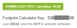 4. Install and run the Calculator, then use your Email and Key (full key displayed on Download page) to activate the Calculator license.  PCB Footprint Expert To get a fully functional Footprint Expert license, complete the Evaluation License request on the Downloads page. Make sure to provide all the requested information, such as your company details and CAD outputs needed. Get your FREE Footprint Calculator or Footprint Expert Evaluation License: Call: 847-557-2300 |
||||||||||||||||||||||||||||||||||||||||||||||||
|
||||||||||||||||||||||||||||||||||||||||||||||||
|
Post Reply
|
|
| Tweet |
| Forum Jump | Forum Permissions You cannot post new topics in this forum You cannot reply to topics in this forum You cannot delete your posts in this forum You cannot edit your posts in this forum You cannot create polls in this forum You cannot vote in polls in this forum |


 Topic Options