What's Wrong with Your Footprint?!
Printed From: PCB Libraries Forum
Category: PCB Footprint Expert
Forum Name: Features & Training
Forum Description: quick-start tips, images, videos, training, and webinars
URL: https://www.PCBLibraries.com/forum/forum_posts.asp?TID=3404
Printed Date: 21 Jun 2026 at 7:56am
Topic: What's Wrong with Your Footprint?!
Posted By: Nick B
Subject: What's Wrong with Your Footprint?!
Date Posted: 31 Jul 2024 at 3:57am
 The
Footprint Expert automates footprints to perfection. Professional,
detailed, and accurate parts – all built consistently with identical rules,
regardless of how many people are involved in your library development. Get your FREE Footprint Calculator or Footprint Expert Evaluation License: https://www.pcblibraries.com/Register" rel="nofollow - https://www.PCBLibraries.com/Register Call us - 847-557-2300 ------------- Stay connected - follow us! https://twitter.com/PCBLibraries" rel="nofollow - X - http://www.linkedin.com/company/pcb-libraries-inc-/" rel="nofollow - LinkedIn |
||||||||||||||||||||||||||||||||||||||||||||||||
Replies:
Posted By: Nick B
Date Posted: 30 Jan 2025 at 12:13pm
|
The free Footprint Calculator and the Footprint Expert are compared here: https://www.pcblibraries.com/products/compare" rel="nofollow - https://www.pcblibraries.com/products/compare To download and use the free Footprint Calculator: 1. Login at https://www.pcblibraries.com/downloads" rel="nofollow - https://www.PCBLibraries.com/downloads (login with existing account, or register for free) 2. If you see this button, click it: 3. If you do not see it, you already have a Key. Click this button to download: 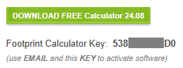 4. Install and run the Calculator, then use your Email and Key (full key displayed on Download page) to activate the Calculator license.  PCB Footprint Expert To get a fully functional Footprint Expert license, complete the Evaluation License request on the Downloads page. Make sure to provide all the requested information, such as your company details and CAD outputs needed. Get your FREE Footprint Calculator or Footprint Expert Evaluation License: https://www.pcblibraries.com/Register" rel="nofollow - https://www.PCBLibraries.com/Register Call: 847-557-2300 ------------- Stay connected - follow us! https://twitter.com/PCBLibraries" rel="nofollow - X - http://www.linkedin.com/company/pcb-libraries-inc-/" rel="nofollow - LinkedIn |