

|
|
Terminal Density Level of BGA footprints |
Post Reply 
|
| Author | |
asdfasdfa 
New User 
Joined: 26 Mar 2019 Status: Offline Points: 4 |
 Post Options Post Options
") Thanks(0) Thanks(0)
 Quote Reply Quote Reply
 Topic: Terminal Density Level of BGA footprints Topic: Terminal Density Level of BGA footprintsPosted: 18 Feb 2022 at 1:17pm |
|
I'm wondering if it's intended that there isn't an option for setting the Density Level on BGA parts, i.e., Least, Nominal, and Most. I can't remember for sure, but I thought in older versions of Footprint Expert you could. I'm working on a tight machine-assembled board, so I've been using Least for all my footprints. I just made a new BGA footprint and the courtyard looks rather large; maybe that is the size the courtyard needs to be. The package of the part is 1.4 by 0.9 mm (it's a small 6 pin logic gate), and the courtyard looks about 4 times the size of the part. On a 0402 resistor it looks like the courtyard is 0.1 mm, but on this part it was about 0.5 mm out. The package family is the TI YZP: https://www.ti.com/lit/ml/mxbg347/mxbg347.pdf
|
|
 |
|

|
|
|
|
|
Tom H
Admin Group 

Joined: 05 Jan 2012 Location: San Diego, CA Status: Offline Points: 6075 |
Post Options
Thanks(0)
Quote Reply
Posted: 18 Feb 2022 at 1:34pm |
|
The 3-tier density levels for BGA are broken down by Ball Diameter and the pad size % reduction.
 You can change the Courtyard setting in "Tools > Options> Terminals > SM Grid Array > BGA" 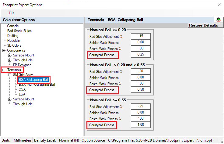 |
|
|
|
|
Post Reply
|
|
| Tweet |
| Forum Jump | Forum Permissions You cannot post new topics in this forum You cannot reply to topics in this forum You cannot delete your posts in this forum You cannot edit your posts in this forum You cannot create polls in this forum You cannot vote in polls in this forum |


 Topic Options