

|
|
Pin 1 dot and placement in Altium |
Post Reply 
|
| Author | |
jnbrown 
Active User 
Joined: 13 Jan 2020 Status: Offline Points: 40 |
 Post Options Post Options
") Thanks(0) Thanks(0)
 Quote Reply Quote Reply
 Topic: Pin 1 dot and placement in Altium Topic: Pin 1 dot and placement in AltiumPosted: 05 Jun 2020 at 9:36am |
|
I have noticed in Altium that the pin 1 dot on the overlay layer causes the Altium bounding box of the part to be extended which prevents placement of components on that side of the IC when using a horizontal clearance rule.
So I end up having to disable the rule using the R key shortcut when placing these parts. I was wondering if there is any way around this. Thanks
|
|
 |
|
|
|
|
|
|
Tom H
Admin Group 

Joined: 05 Jan 2012 Location: San Diego, CA Status: Offline Points: 6075 |
Post Options
Thanks(0)
Quote Reply
Posted: 05 Jun 2020 at 10:41am |
|
Are you referring to the "Automatic" Pin 1 set in Preferences? Let us know so we can fix it.
Or are you referring to the manual insertion of Pin 1 polarity marker? We prefer the manual method because that data is saved to the FPX file and you can easily control the polarity size (small or large depending on the package size), the location and the symbol shape. Also, in the new V2020, manually inserting polarity markings has advanced features that make it easier to add and edit them. Here are the current polarity marking shapes that are available -  Here is the new V2020 "Insert Shape" dialog menu - 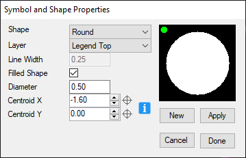 You see the up/down buttons to the left of the coordinates. They are used to move the polarity marker to your desired location. The layers have been expanded to Top and Bottom Legend, Assembly, Solder & Paste Mask. You can stay in the menu and add multiple drafting symbols. The automatic Pin 1 dot feature will by in V2020, but most people will use the manual option. |
|
|
|
|
jnbrown
Active User
Joined: 13 Jan 2020 Status: Offline Points: 40 |
Post Options
Thanks(0)
Quote Reply
Posted: 05 Jun 2020 at 11:32am |
|
Tom,
I believe it is the automatic method. I will try using the manual method. However, I think any pin 1 indicator placed outside the part will push out the bounding box in Altium which causes the problem. I guess one solution is to use a pin 1 indicator that is not outside the footprint.
|
|
|
|
|
Tom H
Admin Group
Joined: 05 Jan 2012 Location: San Diego, CA Status: Offline Points: 6075 |
Post Options
Thanks(0)
Quote Reply
Posted: 05 Jun 2020 at 11:48am |
|
Here is a short video that explains the manual method.
This is preferred by professional PCB designers as they have 100% control of the size, shape, location and layer. The automatic method is not flexible. |
|
|
|
|
jnbrown
Active User
Joined: 13 Jan 2020 Status: Offline Points: 40 |
Post Options
Thanks(0)
Quote Reply
Posted: 05 Jun 2020 at 11:52am |
|
Great!
Thank you
|
|
|
|
|
Post Reply
|
|
| Tweet |
| Forum Jump | Forum Permissions You cannot post new topics in this forum You cannot reply to topics in this forum You cannot delete your posts in this forum You cannot edit your posts in this forum You cannot create polls in this forum You cannot vote in polls in this forum |


 Topic Options