|
|
PCB Design Optimization Starts in the CAD Library |
Post Reply 
|
Page <123> |
| Author | |
budnoel 
Active User 

Joined: 16 Mar 2012 Status: Offline Points: 17 |
 Post Options Post Options
") Thanks(0) Thanks(0)
 Quote Reply Quote Reply
 Posted: 25 Jun 2013 at 5:05am Posted: 25 Jun 2013 at 5:05am |
|
Hello,
|
|
 |
|

|
|
|
|
|
Tom H
Admin Group 

Joined: 05 Jan 2012 Location: San Diego, CA Status: Offline Points: 6075 |
Post Options
Thanks(0)
Quote Reply
Posted: 25 Jun 2013 at 7:03am |
|
There is a "Footprint" tab in the Library Expert that allows the user to enter the mfr. recommended pad size and spacing.
If you open the SM.FPX file you will find that almost all the Oscillators have the mfr. recommended footprint values inserted into the "Footprint" tab in the IPC Calculator. The big thing is the visual alignment of the component leads superimposed on the pad. I try both IPC and Mfr. and the one that physically looks best to me is the one I use. For Side & Corner Concave Oscillators, I personally prefer to use the mfr. recommendation and when I do, that data is stored in the FPX file so when I change Drafting Outline or Ref Des sizes (in the User Preferences) the actual footprint pad placement always comes out the same when I use "Batch Create" to upgrade my entire library with new rules. |
|
|
|
|
wanghai
New User 

Joined: 25 Jun 2013 Location: china Status: Offline Points: 2 |
Post Options
Thanks(0)
Quote Reply
Posted: 25 Jun 2013 at 11:01pm |
|
|
|
|
|
|
Nick B
Admin Group

Joined: 02 Jan 2012 Status: Offline Points: 2020 |
Post Options
Thanks(1)
Quote Reply
Posted: 28 Jun 2013 at 12:50pm |
|
This presentation has been updated!!Just make sure you are logged in to the forum and click this link (same as the link above):
PCB Design Optimization Presentation What was changed: We added some 3D modeling updates - because the Library Expert now also outputs high quality 3D STEP - right with the footprints!! Yes, you don't need to manually create 3D models again!!! See some of the actual output files here. You don't need to manually create footprints or search websites to find a matching 3D model or deal with the quality of a download from a website or the consistency of various 3D models downloaded from different websites. Library Expert puts you in control of your 3D model library to auto-generate 3D models fast and accurate when you need them.
|
|
|
|
|
Nick B
Admin Group
Joined: 02 Jan 2012 Status: Offline Points: 2020 |
Post Options
Thanks(0)
Quote Reply
Posted: 05 Sep 2013 at 9:53pm |
|
This presentation has been updated!!
Just make sure you are logged in to the forum and click this link (same as the link above): PCB Design Optimization Presentation |
|
|
|
|
naik_pushkar
New User
Joined: 31 Jan 2013 Location: INDIA Status: Offline Points: 1 |
Post Options
Thanks(0)
Quote Reply
Posted: 14 Nov 2013 at 4:18am |
|
|
|
|
|
|
Artwork Master ITALY
Active User

Joined: 12 Mar 2012 Location: Milano ITALY Status: Offline Points: 43 |
Post Options
Thanks(0)
Quote Reply
Posted: 10 Jan 2014 at 2:34am |
|
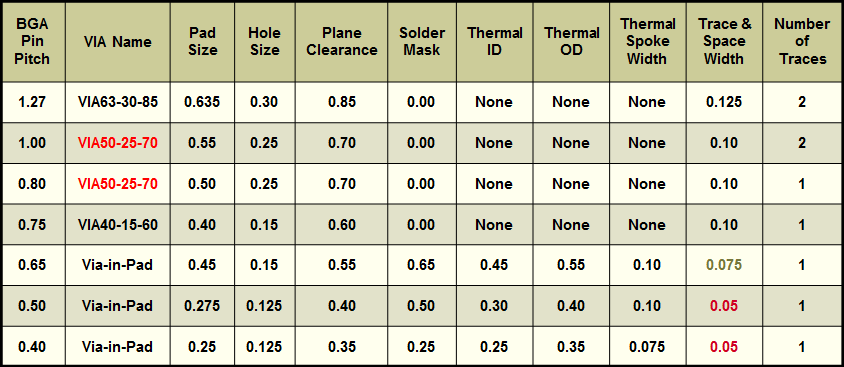
maybe on pag. 25 of the document there is an error on the name of the via for BGA Pin Pitch 1.00 mm
it should be VIA55-25-70 |
|
|
|
|
Tom H
Admin Group
Joined: 05 Jan 2012 Location: San Diego, CA Status: Offline Points: 6075 |
Post Options
Thanks(0)
Quote Reply
Posted: 10 Jan 2014 at 8:11am |
|
This Via table is just the favorites. For the full spreadsheet download padstacks click here The VIA55-25-70 is for a 0.15 mm trace / space (one trace between vias) The VIA50-25-70 is for a 0.10 mm trace / space (two traces between vias)
|
|
|
|
|
Artwork Master ITALY
Active User
Joined: 12 Mar 2012 Location: Milano ITALY Status: Offline Points: 43 |
Post Options
Thanks(0)
Quote Reply
Posted: 10 Jan 2014 at 11:22am |
|
You are correct i was thinking that the VIA Name was based on the dimensions of the PAD but this is wrong.
|
|
|
|
|
wanghai
New User
Joined: 25 Jun 2013 Location: china Status: Offline Points: 2 |
Post Options
Thanks(0)
Quote Reply
Posted: 31 Mar 2014 at 5:21am |
 Thanks! Thanks!
|
|
|
|
|
Post Reply
|
Page <123> |
| Tweet |
| Forum Jump | Forum Permissions You cannot post new topics in this forum You cannot reply to topics in this forum You cannot delete your posts in this forum You cannot edit your posts in this forum You cannot create polls in this forum You cannot vote in polls in this forum |


 Topic Options