PCB Design Optimization Starts in the CAD Library
Printed From: PCB Libraries Forum
Category: Libraries
Forum Name: PCB Library Construction Guidelines
Forum Description: Documentation of the Footprint Expert Guidelines
URL: https://www.PCBLibraries.com/forum/forum_posts.asp?TID=468
Printed Date: 26 Jun 2026 at 1:12am
Topic: PCB Design Optimization Starts in the CAD Library
Posted By: Nick B
Subject: PCB Design Optimization Starts in the CAD Library
Date Posted: 20 Jul 2012 at 9:32am
|
PCB Design Optimization (updated September 5, 2013)
This 149-page Presentation is absolutely FREE!
Just make sure you are logged in to the forum and click this link:
https://www.pcblibraries.com/downloads/Guidelines!PCB_Design_Perfection_Starts_in_the_CAD_Library.asp" rel="nofollow - PCB Design Optimization Presentation (first 25 slides of the 146-slide presentation are shown below)
 The following document represents every Surface Mount component family in the PCB Library Expert with graphic illustrations of every 3D STEP model, example Footprint with Silkscreen and updated Solder Joint Goal Tables: http://www.pcblibraries.com/Products/FPX/UserGuide/download/Library%20Expert%20Surface%20Mount%20Component%20Families.pdf" rel="nofollow - The Library Expert's Surface Mount Component Families ------------- Stay connected - follow us! https://twitter.com/PCBLibraries" rel="nofollow - X - http://www.linkedin.com/company/pcb-libraries-inc-/" rel="nofollow - LinkedIn |
Replies:
Posted By: konraditen
Date Posted: 20 Jul 2012 at 10:52am
|
thanks for the share. Konrad
|
Posted By: Nick B
Date Posted: 20 Jul 2012 at 11:08am
|
No problem at all! Feel free to click  Thanks for posts you like - keeps the forum cleaner. It also gets forum users more points. Thanks for posts you like - keeps the forum cleaner. It also gets forum users more points.  |
Posted By: Nick B
Date Posted: 13 Oct 2012 at 7:32pm
|
This presentation has been updated!! Just make sure you are logged in to the forum and click this link (same as the link above): http://www.pcblibraries.com/downloads/Guidelines%21PCB_Design_Optimization_Starts_in_the_CAD_Library.asp" rel="nofollow - PCB Design Optimization Presentation |
Posted By: tinghai899220
Date Posted: 30 Oct 2012 at 4:38am
| thanks |
Posted By: Blueprint
Date Posted: 07 Jan 2013 at 5:21pm
| Thanks ! |
Posted By: ijossa
Date Posted: 13 Feb 2013 at 9:54am
| Thanks! Very good overview! |
Posted By: rushway
Date Posted: 26 Mar 2013 at 8:37pm
|
Great! This is one of the most excellent document I have read. |
Posted By: budnoel
Date Posted: 17 Jun 2013 at 5:36am
| Hello - We have been creating our standard library component padstacks with a one-to-one relationship between the pad size and the Soldermask size. On our fabrication drawing we then include the following note: "RESIZING FOR OPTIMAL MASK CLEARANCE TO CONDUCTIVE FEATURES PERMISSIBLE." Is this the best approach or should we be internally adjusting our SM to Pad clearances for each design before we release them for fabrication? |
Posted By: Tom H
Date Posted: 17 Jun 2013 at 6:30am
|
You're on the right track. When I tour manufacturing facilities and that question always comes up and the answer is always the same. Please provide all solder mask features 1:1 scale so we have a known starting point to swell the mask to fit your PCB trace/space technology and our fabrication tolerance. "The Solder Mask provided in the Gerber data can be swelled to accomodate your manufacturing tolerances. Do not expose any traces, vias or copper pour." There a many different ways to word this fabrication note, so I would discuss it with the fabrication shop to get their feedback. I have noticed in many CAD tools that they provide a global solder mask swell for pad features, but if you do this, I would also notify fabrication what you did. |
Posted By: budnoel
Date Posted: 25 Jun 2013 at 5:05am
|
Hello, |
Posted By: Tom H
Date Posted: 25 Jun 2013 at 7:03am
|
There is a "Footprint" tab in the Library Expert that allows the user to enter the mfr. recommended pad size and spacing. If you open the SM.FPX file you will find that almost all the Oscillators have the mfr. recommended footprint values inserted into the "Footprint" tab in the IPC Calculator. The big thing is the visual alignment of the component leads superimposed on the pad. I try both IPC and Mfr. and the one that physically looks best to me is the one I use. For Side & Corner Concave Oscillators, I personally prefer to use the mfr. recommendation and when I do, that data is stored in the FPX file so when I change Drafting Outline or Ref Des sizes (in the User Preferences) the actual footprint pad placement always comes out the same when I use "Batch Create" to upgrade my entire library with new rules. ------------- Stay connected - follow us! https://twitter.com/PCBLibraries" rel="nofollow - X - http://www.linkedin.com/company/pcb-libraries-inc-/" rel="nofollow - LinkedIn |
Posted By: wanghai
Date Posted: 25 Jun 2013 at 11:01pm
|
|
Posted By: Nick B
Date Posted: 28 Jun 2013 at 12:50pm
|
This presentation has been updated!!Just make sure you are logged in to the forum and click this link (same as the link above): http://www.pcblibraries.com/downloads/Guidelines%21PCB_Design_Optimization_Starts_in_the_CAD_Library.asp" rel="nofollow - PCB Design Optimization Presentation What was changed: We added some 3D modeling updates - because the Library Expert now also outputs high quality http://www.pcblibraries.com/Products/FPX/3D-STEP.asp" rel="nofollow - 3D STEP - right with the footprints!! Yes, you don't need to manually create 3D models again!!! See some of the actual output files http://www.pcblibraries.com/downloads/Samples_3D_STEP.zip" rel="nofollow - here . You don't need to manually create footprints or search websites to find a matching 3D model or deal with the quality of a download from a website or the consistency of various 3D models downloaded from different websites. Library Expert puts you in control of your 3D model library to auto-generate 3D models fast and accurate when you need them.
------------- Stay connected - follow us! https://twitter.com/PCBLibraries" rel="nofollow - X - http://www.linkedin.com/company/pcb-libraries-inc-/" rel="nofollow - LinkedIn |
Posted By: Nick B
Date Posted: 05 Sep 2013 at 9:53pm
|
This presentation has been updated!! Just make sure you are logged in to the forum and click this link (same as the link above): http://www.pcblibraries.com/downloads/Guidelines%21PCB_Design_Optimization_Starts_in_the_CAD_Library.asp" rel="nofollow - PCB Design Optimization Presentation ------------- Stay connected - follow us! https://twitter.com/PCBLibraries" rel="nofollow - X - http://www.linkedin.com/company/pcb-libraries-inc-/" rel="nofollow - LinkedIn |
Posted By: naik_pushkar
Date Posted: 14 Nov 2013 at 4:18am
|
|
Posted By: Artwork Master ITALY
Date Posted: 10 Jan 2014 at 2:34am
|
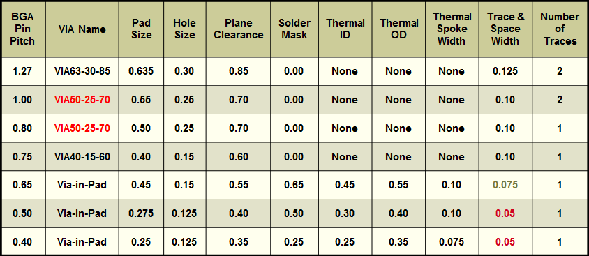
maybe on pag. 25 of the document there is an error on the name of the via for BGA Pin Pitch 1.00 mm it should be VIA55-25-70 |
Posted By: Tom H
Date Posted: 10 Jan 2014 at 8:11am
|
This Via table is just the favorites. For the full spreadsheet download padstacks click http://www.pcblibraries.com/forum/proportional-throughhole-padstacks_topic90.html" rel="nofollow - here The VIA55-25-70 is for a 0.15 mm trace / space (one trace between vias) The VIA50-25-70 is for a 0.10 mm trace / space (two traces between vias)
------------- Stay connected - follow us! https://twitter.com/PCBLibraries" rel="nofollow - X - http://www.linkedin.com/company/pcb-libraries-inc-/" rel="nofollow - LinkedIn |

Posted By: Artwork Master ITALY
Date Posted: 10 Jan 2014 at 11:22am
|
You are correct i was thinking that the VIA Name was based on the dimensions of the PAD but this is wrong. |
Posted By: wanghai
Date Posted: 31 Mar 2014 at 5:21am
 Thanks! Thanks!
|
Posted By: bnoel
Date Posted: 25 Apr 2014 at 4:11am
| Hello - What determines whether a pad is rectangular in shape versus oblong? |
Posted By: Tom H
Date Posted: 25 Apr 2014 at 6:40am
|
IPC-7351 says that the preferred SMT pad shape should be oblong or rounded rectangle if your CAD tool supports that feature. Every component manufacturer recommends rectangular pad shape. i.e.: I've never seen a mfr. recommended footprint with oblong pad shape. PCB Libraries, Inc. recommends D-shape pads for QFN & PQFN and Rounded Rectangle for every other surface mount pad (including Chip components). Rounded Rectangle in the pad shape of the future, where IPC and the component manufacturer can both agree on that. ------------- Stay connected - follow us! https://twitter.com/PCBLibraries" rel="nofollow - X - http://www.linkedin.com/company/pcb-libraries-inc-/" rel="nofollow - LinkedIn |
Posted By: Artwork Master ITALY
Date Posted: 25 Apr 2014 at 7:44am
| You mean "Rounded Rectangle is the pad shape of the future" |
Posted By: Tom H
Date Posted: 25 Apr 2014 at 7:47am
|
Yes, in the year 2017 most PCB designers will use "Rounded Rectangle" pad shape for surface mount footprints. It meets IPC and the component manufacturers 1/2 way. IPC = Oblong pad shape Component Mfr. = Rectangle pad shape Future = Rounded Rectangle pad shape ------------- Stay connected - follow us! https://twitter.com/PCBLibraries" rel="nofollow - X - http://www.linkedin.com/company/pcb-libraries-inc-/" rel="nofollow - LinkedIn |
Posted By: Matthew Lamkin
Date Posted: 29 Apr 2014 at 8:11am
|
The reason for using the Rounded rectangle pads is because now that most are using lead free solder, they are finding that it does not flow into the corners so rectangular pads are no longer needed. Although I wouldn't say "most" are actually using them, a great many I see are still using rectangular ones and mixing them up with rounded rectangles upsets them |
Posted By: Nick B
Date Posted: 21 Aug 2014 at 8:52am
|
This document represents every Surface Mount component family in the PCB Library Expert with graphic illustrations of every 3D STEP model, example Footprint with Silkscreen and updated Solder Joint Goal Tables. http://www.pcblibraries.com/Products/FPX/UserGuide/download/Surface%20Mount%20Component%20Families%20for%20IPC%20Calculator.pdf" rel="nofollow - The Library Expert's Surface Mount Component Families ------------- Stay connected - follow us! https://twitter.com/PCBLibraries" rel="nofollow - X - http://www.linkedin.com/company/pcb-libraries-inc-/" rel="nofollow - LinkedIn |
Posted By: tjnash75
Date Posted: 10 Sep 2021 at 5:49am
|
In the presentation associated with this thread, Tom makes the statement "I would not recommend building Footprints using Metric Units for Inch based PCB design layout. The pad size, drafting items, feature spacing & round-off values are not compatible. Inch design = Inch libraries & Metric design = Metric libraries". If I recall, on another occasion Tom mentioned PCB fab houses having to translate everything to imperial units. So, what is the current guidance? It sounds like if we go completely metric (library and PCB design, it complicates fab. And if we go completely imperial for library and PCB design, it sounds like we're running counter to the advice of the IPC. We have traditionally done our PCB designs in imperial units. That would imply, based on the guidance above, we should be doing the footprints in imperial units as well. Where the heck do we go from here???
|
Posted By: Tom H
Date Posted: 10 Sep 2021 at 9:26am
|
The entire electronics industry needs to convert to metric units for both PCB libraries and PCB design. People who are still using Imperial units are holding the industry back in the stone age. My personal challenge for everyone using Imperial Units is to do everything in millimeters for 5 PCB layouts. Once you find out the superiority of the metric system, you will never go back to Imperial Units. It's a short learning curve but it's worth it. ------------- Stay connected - follow us! https://twitter.com/PCBLibraries" rel="nofollow - X - http://www.linkedin.com/company/pcb-libraries-inc-/" rel="nofollow - LinkedIn |
Posted By: MCERQUE4
Date Posted: 28 Mar 2024 at 9:29am
|
Thanks for share this information! |
Posted By: WilliamsimC
Date Posted: 19 Apr 2024 at 2:45am
|
Starting to make the PCB design better begins with the CAD library. This is where we keep all the parts we'll use to build the design. Making sure these parts are right is super important because they're like the building blocks of our project. When we pick and set up the parts in the library, it helps us make the design process smoother, fix any signal problems, and stop mistakes early on. Also, having a neat CAD library helps us keep things consistent in our designs, lets us reuse parts that work well, and makes it easier for us to work together as a team. So, spending time to make sure our CAD library is in good shape is a smart move for making awesome PCB designs.
|