

|
|
JEDEC Standard Footprints? |
Post Reply 
|
| Author | |
craig4tone 
Advanced User 
Joined: 29 Nov 2016 Status: Offline Points: 95 |
 Post Options Post Options
") Thanks(0) Thanks(0)
 Quote Reply Quote Reply
 Topic: JEDEC Standard Footprints? Topic: JEDEC Standard Footprints?Posted: 23 Jan 2017 at 11:53am |
|
To precursor the discussion, I have been involved in PCB and ECAD Management for 25+ years. I have worked exclusively as a Manager for Library Services company in the past and have seen it all both good and bad.
I am now working for a service-based company and we purchased Library Expert in order to maintain a centralized component database that we can export to various toolflows and with various settings (IPC-7351C vs. customer-specific, etc.) In my experience, there is little merit in creating 20 variations of an SOIC-8 (3.9mm width) per manufacturer. This only serves to make the library confusing as well as create potential problems with PCB re-use in the case of obsolescence. I.e. TI disco's a PN and On Semi has a replacement but the "recommended pads" or tolerancing creates a wider IPC-7351C pattern that creates a DRC if replaced and the PCB MUST remain the same for compliance reasons (UL, FCC, etc.). I also have "friends" that work for un-named chip vendors and the "recommended footprints" and package drawings are most often a joke as the datasheets are created by interns and that info is often copy/pasted from unknown sources and/or Google.  With that being said, where can I find JEDEC package mechanical drawings to build parametric libraries from? I am thinking of standardizing things such as SOT, SOIC, chip components, molded body caps, SM* diodes, etc. What if any standardization of footprints have any of you attempted? I'm even toying with the idea of combining resistor and cap 0402 into a single "RC0402" package with a worst case ceramic cap height.
|
|
 |
|
|
|
|
Tom H
Admin Group 

Joined: 05 Jan 2012 Location: San Diego, CA Status: Offline Points: 5716 |
Post Options
Thanks(0)
Quote Reply
Posted: 23 Jan 2017 at 12:03pm |
|
For the standard JEDEC package dimensions - http://www.jedec.org/ However, very few mfr.'s use these. SOIC = MO-059, -099, -119, -120 SOP40 = MO-154 SOP65 = MO-150 Just register on JEDEC.org and download all MS, MO, DO and TO PDF files. |
|
|
|
|
craig4tone
Advanced User
Joined: 29 Nov 2016 Status: Offline Points: 95 |
Post Options
Thanks(0)
Quote Reply
Posted: 23 Jan 2017 at 12:14pm |
|
Thanks for the JEDEC info ... I just assumed is was pay-to-play like IEEE papers. The parts are created at an IC packaging facility of which several manufacturer's share the same facilities and SOT, SOIC, TSSOP, etc. are all built to JEDEC standards because of existing tooling that was created back when SMT adopted the standards. Granted, the newer, unique packages such as the PDSON-8, thermal pad devices, etc. are the exception to that rule, but I am referring to the "industry standard" parts like 0402 resistors, SOT23-3, SOT23-5, SOIC8, SOIC8W, SMA, SMB, SMC, EIA molded body, etc.
|
|
|
|
|
Tom H
Admin Group
Joined: 05 Jan 2012 Location: San Diego, CA Status: Offline Points: 5716 |
Post Options
Thanks(0)
Quote Reply
Posted: 23 Jan 2017 at 12:18pm |
|
When you download the JEDEC datasheets and look at the package dimensions, try to match them with your mfr.'s package dimensions. You will find out that they are close but not a direct match. I think that mfr.'s need to pay JEDEC a royalty if they use their package dimensions. Therefore they change them slightly. But I agree with you in that one SOIC8 footprint should be good for all, but only if the package dimensions are within a 0.20 mm tolerance of each other. |
|
|
|
|
Louis_Guerin
Active User 

Joined: 29 Jan 2013 Location: Quebec Status: Offline Points: 24 |
Post Options
Thanks(0)
Quote Reply
Posted: 23 Jan 2017 at 12:21pm |
|
JEDEC pacjkage are on http://www.jedec.org/category/technology-focus-area/jc-10/registered-outlines-jep95
As Tom mentionned you have to register to have them. As for the RC0402 I've though of it once, however PCB patterns cap are a bit wider than resistors because of sides that can be soldered which is not the case for resistors and in some case this extra surface could cause placement problem on crowded PCB. Of course you can use the resistor pattern for both of them but then why cap have component end covered on all side and not the resistor? Could somebody enlight us on this?
 |
|
|
|
|
Tom H
Admin Group
Joined: 05 Jan 2012 Location: San Diego, CA Status: Offline Points: 5716 |
Post Options
Thanks(0)
Quote Reply
Posted: 23 Jan 2017 at 12:46pm |
|
You need separate Chip land patterns for Capacitors and Resistors.
Capacitors should have a side fillet and Resistors do not. However, IPC says that the same pattern can be used for both because the Side Fillet is not required per IPC-J-STD-001. They do mention in Note 3 that there should be "Visible Wetting" but that's not possible with chips that do not have a terminal lead wraparound.  Here are 3D models created by Library Expert Pro. 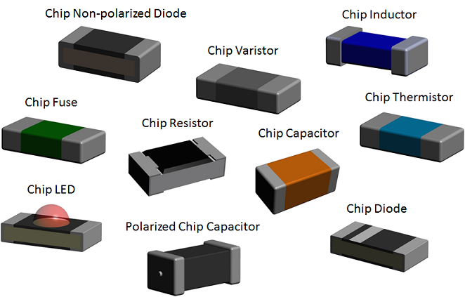 |
|
|
|
|
Post Reply
|
|
| Tweet |
| Forum Jump | Forum Permissions You cannot post new topics in this forum You cannot reply to topics in this forum You cannot delete your posts in this forum You cannot edit your posts in this forum You cannot create polls in this forum You cannot vote in polls in this forum |


 Topic Options