

|
|
Chips: Add More Types of Silkscreens |
Post Reply 
|
Page 12> |
| Author | |
pzt648485640 
Advanced User 

Joined: 02 Aug 2013 Location: shanghai Status: Offline Points: 90 |
 Post Options Post Options
") Thanks(0) Thanks(0)
 Quote Reply Quote Reply
 Topic: Chips: Add More Types of Silkscreens Topic: Chips: Add More Types of SilkscreensPosted: 18 Dec 2021 at 10:55am |
|
No matter what Chip is selected; the silk screen has not been changed; I think it needs to be improved; although the software supports manual addition; the operation is too troublesome! For example, as shown below:   |
|
 |
|

|
|
|
|
|
Tom H
Admin Group 

Joined: 05 Jan 2012 Location: San Diego, CA Status: Offline Points: 6074 |
Post Options
Thanks(0)
Quote Reply
Posted: 18 Dec 2021 at 11:03am |
|
Many users have 2 FPX files.
One for adding the Calculator dimensions for 3D STEP creation. One for moving the footprint to FP Designer to get a full body silkscreen. |
|
|
|
|
pzt648485640
Advanced User
Joined: 02 Aug 2013 Location: shanghai Status: Offline Points: 90 |
Post Options
Thanks(0)
Quote Reply
Posted: 18 Dec 2021 at 11:41am |
|
I think this is very troublesome; for example, the silk screen rounded corner effect; currently it can only be exported and do the silk screen processing separately; but different platforms...
For example, some require PIN 1 foot silkscreen; some do not; this requires multiple .fpx classification and batch export; this problem still lies in the software design; if some configurations can be saved separately to fpx, it will not require multiple fpx problems .
|
|
|
|
|
pzt648485640
Advanced User
Joined: 02 Aug 2013 Location: shanghai Status: Offline Points: 90 |
Post Options
Thanks(0)
Quote Reply
Posted: 18 Dec 2021 at 11:47am |
|
I think the best way to make silk screen is to define it once by the user; apply the formula to calculate it directly later; instead of designing the silk screen for the same type of component multiple times.
|
|
|
|
|
Tom H
Admin Group
Joined: 05 Jan 2012 Location: San Diego, CA Status: Offline Points: 6074 |
Post Options
Thanks(0)
Quote Reply
Posted: 18 Dec 2021 at 11:54am |
|
We'll look into this as an Option that is applied when you open a footprint.
It can't be saved to FPX file because we're opening a new PCBPOD.com website in January that will have 4 million parts that include schematic symbols, footprints and 3D models. This has been in development for the past 2.5 years. The number of parts will double in 2022 and double again in 2023. Can't change the FPX file at this point, but we can add Options. |
|
|
|
|
pzt648485640
Advanced User
Joined: 02 Aug 2013 Location: shanghai Status: Offline Points: 90 |
Post Options
Thanks(0)
Quote Reply
Posted: 18 Dec 2021 at 12:21pm |
|
There are still quite a lot of online libraries; each has its own characteristics; it does not get a unified standard; and secondly, the management is too cumbersome.
Chip can be solved by setting different types of silk screens for different types... You can refer to the solidworks formula calculation method to follow up a better solution; relying on Footprint to Designer too much is not a long-term solution... |
|
|
|
|
Tom H
Admin Group
Joined: 05 Jan 2012 Location: San Diego, CA Status: Offline Points: 6074 |
Post Options
Thanks(0)
Quote Reply
Posted: 04 Jan 2022 at 3:02pm |
|
We added the silkscreen outline that you recommended for all chips that could not otherwise produce a silkscreen outline due to a user Option Rules violation.
Download and install the V2022.01 pre-release - www.pcblibraries.com/downloads Here is what it looks like: 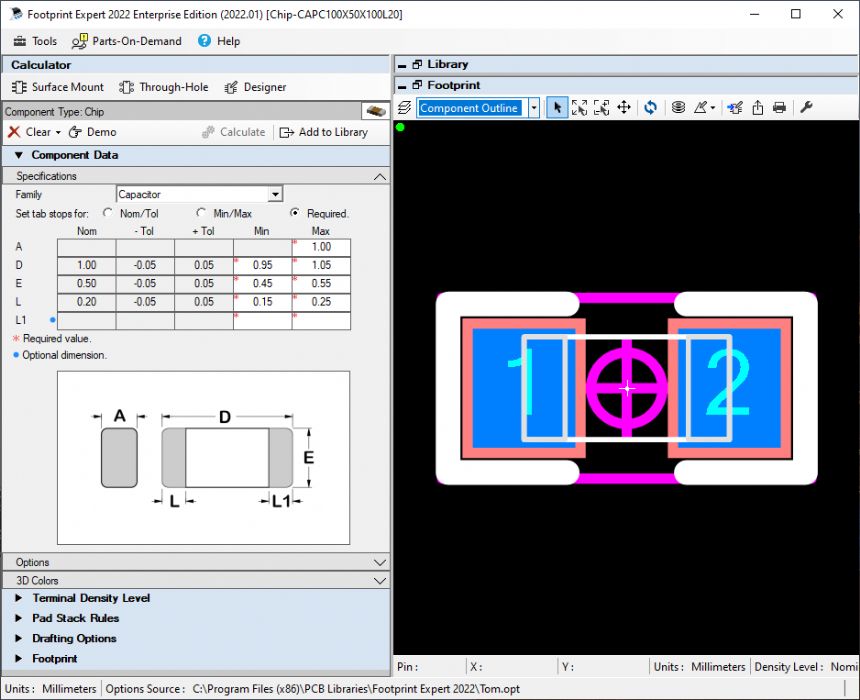 |
|
|
|
|
pzt648485640
Advanced User
Joined: 02 Aug 2013 Location: shanghai Status: Offline Points: 90 |
Post Options
Thanks(0)
Quote Reply
Posted: 07 Jan 2022 at 7:19pm |
|
It is recommended to also add the rectangle to the options.

|
|
|
|
|
Tom H
Admin Group
Joined: 05 Jan 2012 Location: San Diego, CA Status: Offline Points: 6074 |
Post Options
Thanks(0)
Quote Reply
Posted: 08 Jan 2022 at 10:00am |
|
No, it's automatic. All chips will get the line but if the chip is too small for the line it will hatch.
i.e.: every chip will have a silkscreen outline now. Thanks for the idea. |
|
|
|
|
pzt648485640
Advanced User
Joined: 02 Aug 2013 Location: shanghai Status: Offline Points: 90 |
Post Options
Thanks(0)
Quote Reply
Posted: 04 Feb 2022 at 9:50am |
|
Please test other parameters;The value "min" of D cannot be greater than 1.87 to be valid; this modification is a bit wrong! |
|
|
|
|
Post Reply
|
Page 12> |
| Tweet |
| Forum Jump | Forum Permissions You cannot post new topics in this forum You cannot reply to topics in this forum You cannot delete your posts in this forum You cannot edit your posts in this forum You cannot create polls in this forum You cannot vote in polls in this forum |


 Topic Options