

|
|
Altium 0402 Resistor Footprint |
Post Reply 
|
Page <12 |
| Author | |
jnbrown 
Active User 
Joined: 13 Jan 2020 Status: Offline Points: 40 |
 Post Options Post Options
") Thanks(0) Thanks(0)
 Quote Reply Quote Reply
 Posted: 14 Jan 2020 at 3:53pm Posted: 14 Jan 2020 at 3:53pm |
|
I am noticing that in Library Expert Pro the pad corner radius is set to 25%,
but when I import the footprint the radius ends up being 50% in Altium. However looking at footprints the radius looks the same in both programs. Why is the radius value not the same in both programs? |
|
 |
|

|
|
|
|
|
Tom H
Admin Group 

Joined: 05 Jan 2012 Location: San Diego, CA Status: Offline Points: 6075 |
Post Options
Thanks(0)
Quote Reply
Posted: 14 Jan 2020 at 3:58pm |
|
It's 25% per corner or 50% overall.
You can adjust the Corner Radius in the "Rules" tab.
|
|
|
|
|
ransonjd
Committee 
Joined: 15 Nov 2016 Status: Offline Points: 144 |
Post Options
Thanks(0)
Quote Reply
Posted: 27 Feb 2020 at 10:39am |
|
I don't know if it's still an issue, but as of 17.1, the Altium
IPC Wizard didn't follow the IPC standard for the spacing between pads
on chip components. This was what I found and filed with them 3 years
ago:
"Altium is setting the spacing between pads based on the minimum
length of the component, minus twice the maximum band width of the
component. The correct spacing between pads should be based on the nominal length of the component, minus twice the nominal band width of the component, minus the RMS sum of tolerances. This is per section 3.1.1 of IPC-7351." |
|
|
|
|
LaserAlex
Active User

Joined: 06 Jun 2012 Location: Seattle, WA Status: Offline Points: 27 |
Post Options
Thanks(0)
Quote Reply
Posted: 27 Feb 2020 at 10:46am |
Yet another reason to use PCB Library Expert instead of the Wizard in Altium.
|
|
|
|
|
ransonjd
Committee
Joined: 15 Nov 2016 Status: Offline Points: 144 |
Post Options
Thanks(0)
Quote Reply
Posted: 27 Feb 2020 at 10:58am |
|
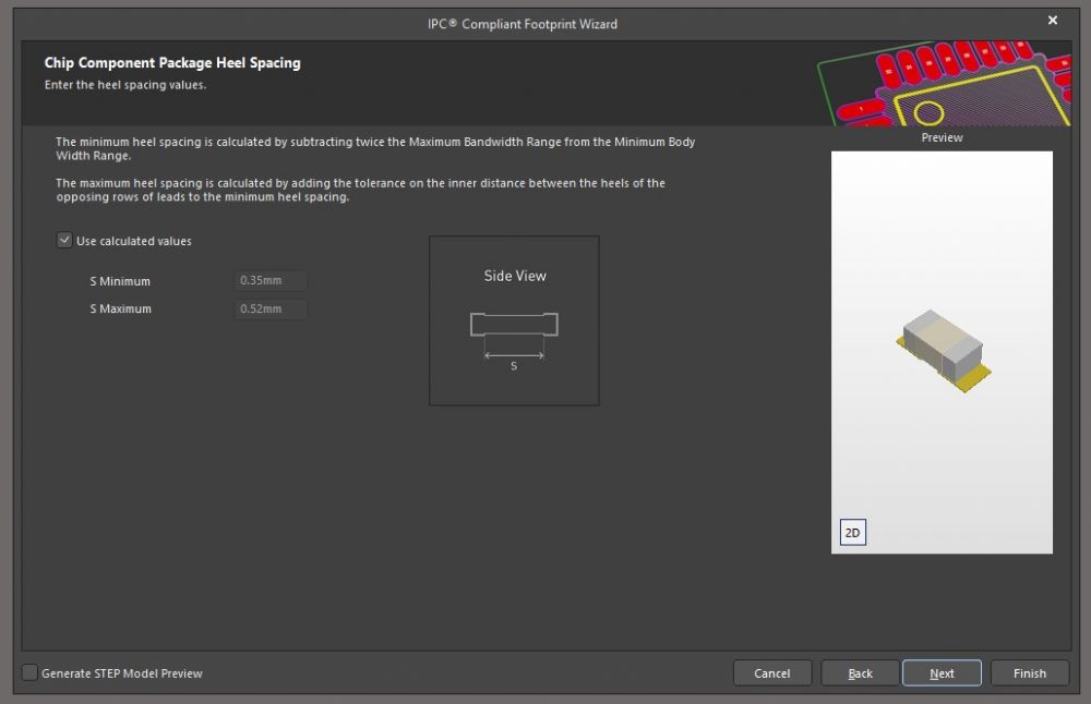
It looks like V20 still uses what I believe is the wrong formula for minimum heel spacing. Tom, can you verify that the minimum heel spacing calculation is not calculated by "subtracting twice the Maximum Bandwidth Range from the Minimum Body Width Range."? |
|
|
|
|
ransonjd
Committee
Joined: 15 Nov 2016 Status: Offline Points: 144 |
Post Options
Thanks(0)
Quote Reply
Posted: 27 Feb 2020 at 11:01am |
|
|
|
|
|
Tom H
Admin Group
Joined: 05 Jan 2012 Location: San Diego, CA Status: Offline Points: 6075 |
Post Options
Thanks(0)
Quote Reply
Posted: 27 Feb 2020 at 11:14am |
|
I did hear about this issue, but everyone should know that Land Pattern Calculators are very complex to create and then you must maintain them as new technology emerges. And we do that every day.
In the case of Altium, in 2005 when they created the Altium Footprint Wizard, the 0201 and 01005 packages were not even on the market yet and the 0402 was brand new. Every chip package size requires a different solder joint goal and even IPC-7351 does not support that theory. But it's true. There are documents on your computer in this folder - C:\Program Files (x86)\PCB Libraries\Library Expert 2019\Documents
These are the Library Expert default solder joint goals as tested and approved by the 100,000 users of Library Expert worldwide. They are all User definable in Preferences and everyone has the right to edit the default values to work best for you. IPC-7351 has been downgraded to a Guideline because even IPC and their Land Pattern Committee doesn't know anymore what solder joint values are best for each terminal lead style. Micro-miniaturization of component packages are changing everything and it's hard for everyone to keep up unless you are 100% dedicated to do so. And PCB Libraries, Inc. is 100% focused on Land Pattern technology. Yesterday, Today and Tomorrow. |
|
|
|
|
Tom H
Admin Group
Joined: 05 Jan 2012 Location: San Diego, CA Status: Offline Points: 6075 |
Post Options
Thanks(0)
Quote Reply
Posted: 27 Feb 2020 at 11:27am |
|
I don't understand why anyone would use the Altium Footprint Wizard when we give away a Free Library Expert Pro that supports 25 CAD tools and produces perfect high quality 3D STEP models simultaneously.
|
|
|
|
|
Post Reply
|
Page <12 |
| Tweet |
| Forum Jump | Forum Permissions You cannot post new topics in this forum You cannot reply to topics in this forum You cannot delete your posts in this forum You cannot edit your posts in this forum You cannot create polls in this forum You cannot vote in polls in this forum |


 Topic Options
 ransonjd wrote: