Altium 0402 Resistor Footprint
Printed From: PCB Libraries Forum
Category: Libraries
Forum Name: Altium
Forum Description:
URL: https://www.PCBLibraries.com/forum/forum_posts.asp?TID=2596
Printed Date: 26 Jun 2026 at 1:12am
Topic: Altium 0402 Resistor Footprint
Posted By: jnbrown
Subject: Altium 0402 Resistor Footprint
Date Posted: 13 Jan 2020 at 10:25am
|
I just started using Altium having previously used PADS. When using the IPC Compliant footprint wizard (medium density) using the dimension from Vishay CRCW data sheet I get the following footprint dimensions: a: 0.55 b: 0.65 I: 0.2 The recommended dimensions from the Vishay datasheet are: a: 0.40 b: 0.60 I: 0.5 The dimension from our PADS library are: a: 0.57 b: 0.62 I: 0.39 It seems that the "I" dimension (spacing between pads) is a lot smaller using the Altium wizard compared to the Vishay datasheet and current PADS library. I asked our contract assembler and they said to use the Altium footprint as it will result in less tombstoning. Would appreciate any opinions on this. Thanks |
Replies:
Posted By: Tom H
Date Posted: 13 Jan 2020 at 12:05pm
|
When I use the Free Library Expert Pro "Nominal Density Level" I get these dimensions: a: 0.55 b: 0.58 I: 0.40 Datasheet: https://www.mouser.com/datasheet/2/427/dcrcw-72725.pdf" rel="nofollow - https://www.mouser.com/datasheet/2/427/dcrcw-72725.pdf The PADS library parts seems to be the closest match. However, the PADS b: dimension is slightly large because there is no metal on the side of a resistor terminal and the package Width Tolerance is only +/- 0.05 mm. The part is 1.00 mm long with a 0.50 mm gap (between two 0.25 mm lead widths). The Altium I: dimension of 0.20 mm is too close and the heel joint would be 0.15 mm. Way out of line and I don't know why the assembly shop would recommend that one. The Library Expert Pro heel joint is 0.05 mm to cover the terminal tolerance. Download the Free (no license required) Library Expert Pro and use the Altium interface to produce an accurate footprint and High Quality 3D STEP model - http://www.pcblibraries.com/LibraryExpert/Pro/" rel="nofollow - http://www.pcblibraries.com/LibraryExpert/Pro/ Library Expert Pro actually shows you the package and terminal outlines on the pad so you can visually see where the solder is going to flow. And the body and terminal are translated to Altium on a mechanical layer. ------------- Stay connected - follow us! https://twitter.com/PCBLibraries" rel="nofollow - X - http://www.linkedin.com/company/pcb-libraries-inc-/" rel="nofollow - LinkedIn |
Posted By: jnbrown
Date Posted: 13 Jan 2020 at 3:43pm
|
Tom, Thanks for the great advice. It is kind of disappointing that our assembler does not know what a proper footprint is. The wizard in Altium has many options, maybe if I select the right ones I would get a footprint that makes more sense. I will give Library Expert Pro a try. |
Posted By: jnbrown
Date Posted: 13 Jan 2020 at 4:19pm
|
When I run it with the numbers from the datasheet I get slightly different results: a: 0.58 b: 0.60 I: 0.35 Not sure why it is different from your results but not a long way off. Also are the rounded corners (set to 25% of pad width) preferred to square corners? Thanks
|
Posted By: Tom H
Date Posted: 13 Jan 2020 at 4:40pm
|
Are these the same package dimensions and tolerances? The tolerances are important. 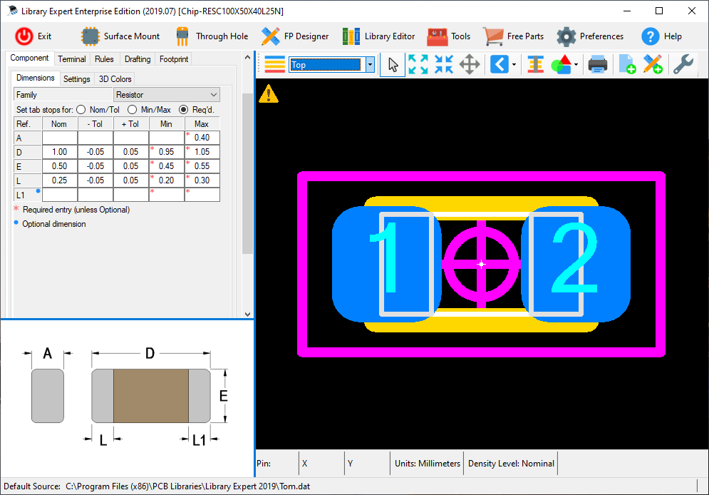 I get these results. If your results are different, we need to talk. 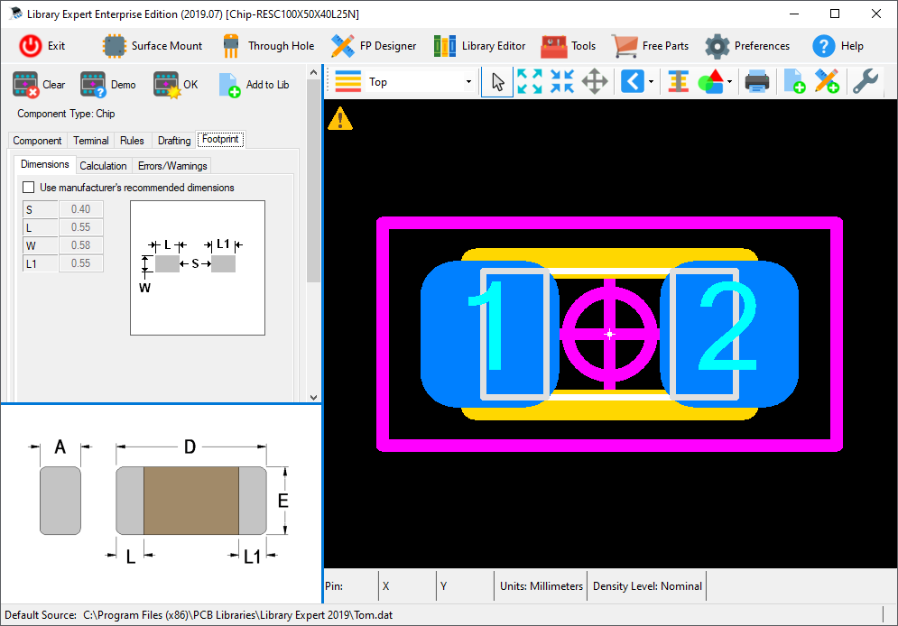 ------------- Stay connected - follow us! https://twitter.com/PCBLibraries" rel="nofollow - X - http://www.linkedin.com/company/pcb-libraries-inc-/" rel="nofollow - LinkedIn |
Posted By: jnbrown
Date Posted: 13 Jan 2020 at 5:22pm
|
Tom, Using the numbers from the datasheet you posted the link to I do indeed get the same numbers as you. Vishay has a lot of versions of the CRCW datasheet. Here is the one I am using that matches the P/N I am using: http://www.vishay.com/docs/28773/crcwce3.pdf" rel="nofollow - http://www.vishay.com/docs/28773/crcwce3.pdf The tolerances are different and it is dated 02-Nov-17. The one you posted the link to is dated 18-Nov-10 Also we have Stackpole as a second source, fortunately their dimensions match Vishay except the tolerance on the termination width is 0.15mm instead of 0.1mm for Vishay.
|
Posted By: Tom H
Date Posted: 13 Jan 2020 at 5:46pm
|
Yep, in the IPC world, the tolerances change the pattern when using the same Nominal Package Dimensions. They are part of the mathematical model. Read this: https://www.pcblibraries.com/forum/ipcjstd001-chip-component-solder-joints_topic2588.html" rel="nofollow - https://www.pcblibraries.com/forum/ipcjstd001-chip-component-solder-joints_topic2588.html For additional info on a popular lead form: https://www.pcblibraries.com/forum/ipcjstd001-gull-wing-leads-and-solder-joints_topic2587.html" rel="nofollow - https://www.pcblibraries.com/forum/ipcjstd001-gull-wing-leads-and-solder-joints_topic2587.html ------------- Stay connected - follow us! https://twitter.com/PCBLibraries" rel="nofollow - X - http://www.linkedin.com/company/pcb-libraries-inc-/" rel="nofollow - LinkedIn |
Posted By: jnbrown
Date Posted: 13 Jan 2020 at 6:11pm
|
I will look at those forum posts. Thanks again! |
Posted By: jnbrown
Date Posted: 14 Jan 2020 at 3:15pm
Tom, Those links do not seem to be working. Would still like to read those. Thanks
|
 Tom H wrote:
Posted By: Tom H
Date Posted: 14 Jan 2020 at 3:20pm
|
I updated the links. ------------- Stay connected - follow us! https://twitter.com/PCBLibraries" rel="nofollow - X - http://www.linkedin.com/company/pcb-libraries-inc-/" rel="nofollow - LinkedIn |
Posted By: jnbrown
Date Posted: 14 Jan 2020 at 3:53pm
|
I am noticing that in Library Expert Pro the pad corner radius is set to 25%, but when I import the footprint the radius ends up being 50% in Altium. However looking at footprints the radius looks the same in both programs. Why is the radius value not the same in both programs? |
Posted By: Tom H
Date Posted: 14 Jan 2020 at 3:58pm
|
It's 25% per corner or 50% overall. You can adjust the Corner Radius in the "Rules" tab.
------------- Stay connected - follow us! https://twitter.com/PCBLibraries" rel="nofollow - X - http://www.linkedin.com/company/pcb-libraries-inc-/" rel="nofollow - LinkedIn |
Posted By: ransonjd
Date Posted: 27 Feb 2020 at 10:39am
|
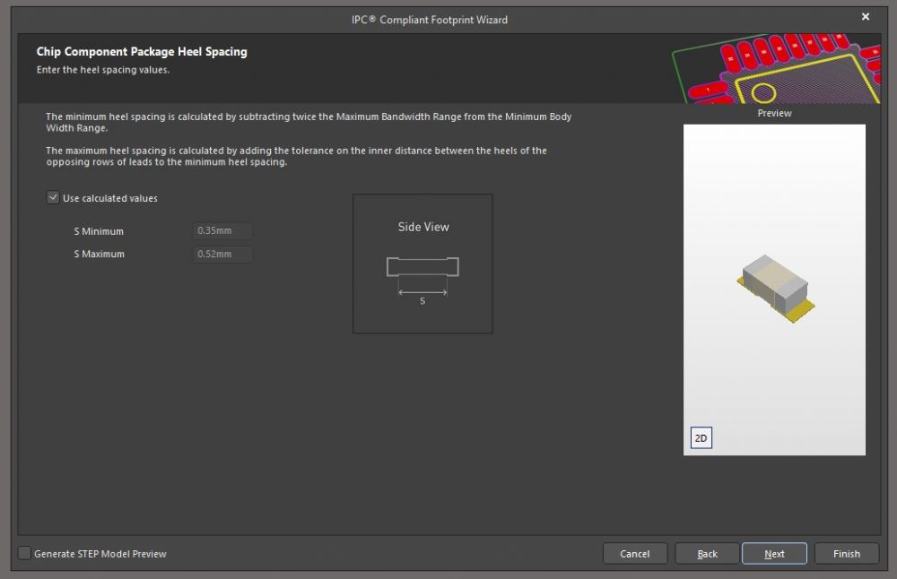
I don't know if it's still an issue, but as of 17.1, the Altium
IPC Wizard didn't follow the IPC standard for the spacing between pads
on chip components. This was what I found and filed with them 3 years
ago: "Altium is setting the spacing between pads based on the minimum
length of the component, minus twice the maximum band width of the
component. The correct spacing between pads should be based on the nominal length of the component, minus twice the nominal band width of the component, minus the RMS sum of tolerances. This is per section 3.1.1 of IPC-7351." |
Posted By: LaserAlex
Date Posted: 27 Feb 2020 at 10:46am
Yet another reason to use PCB Library Expert instead of the Wizard in Altium.
|
Posted By: ransonjd
Date Posted: 27 Feb 2020 at 10:58am
|
It looks like V20 still uses what I believe is the wrong formula for minimum heel spacing. Tom, can you verify that the minimum heel spacing calculation is not calculated by "subtracting twice the Maximum Bandwidth Range from the Minimum Body Width Range."? |
Posted By: ransonjd
Date Posted: 27 Feb 2020 at 11:01am
|
Posted By: Tom H
Date Posted: 27 Feb 2020 at 11:14am
|
I did hear about this issue, but everyone should know that Land Pattern Calculators are very complex to create and then you must maintain them as new technology emerges. And we do that every day. In the case of Altium, in 2005 when they created the Altium Footprint Wizard, the 0201 and 01005 packages were not even on the market yet and the 0402 was brand new. Every chip package size requires a different solder joint goal and even IPC-7351 does not support that theory. But it's true. There are documents on your computer in this folder - C:\Program Files (x86)\PCB Libraries\Library Expert 2019\Documents
These are the Library Expert default solder joint goals as tested and approved by the 100,000 users of Library Expert worldwide. They are all User definable in Preferences and everyone has the right to edit the default values to work best for you. IPC-7351 has been downgraded to a Guideline because even IPC and their Land Pattern Committee doesn't know anymore what solder joint values are best for each terminal lead style. Micro-miniaturization of component packages are changing everything and it's hard for everyone to keep up unless you are 100% dedicated to do so. And PCB Libraries, Inc. is 100% focused on Land Pattern technology. Yesterday, Today and Tomorrow. ------------- Stay connected - follow us! https://twitter.com/PCBLibraries" rel="nofollow - X - http://www.linkedin.com/company/pcb-libraries-inc-/" rel="nofollow - LinkedIn |
Posted By: Tom H
Date Posted: 27 Feb 2020 at 11:27am
|
I don't understand why anyone would use the Altium Footprint Wizard when we give away a Free Library Expert Pro that supports 25 CAD tools and produces perfect high quality 3D STEP models simultaneously. http://www.pcblibraries.com/LibraryExpert/Pro/" rel="nofollow - http://www.pcblibraries.com/LibraryExpert/Pro/ ------------- Stay connected - follow us! https://twitter.com/PCBLibraries" rel="nofollow - X - http://www.linkedin.com/company/pcb-libraries-inc-/" rel="nofollow - LinkedIn |