
 |

|
Thermal Tab Vias |
Post Reply 
|
| Author | |
michaelhallin 
New User 
Joined: 14 Jan 2013 Location: Denmark Status: Offline Points: 3 |
 Post Options Post Options
 Thanks(0) Thanks(0)
 Quote Quote  Reply Reply
 Topic: Thermal Tab Vias Topic: Thermal Tab ViasPosted: 25 Oct 2013 at 1:33am |
|
How can I create a number of vias in the thermal tab of a PowerSO36?
http://www.st.com/st-web-ui/static/active/en/resource/technical/document/datasheet/CD00002294.pdf |
|
 |
|

|
|
 |
|
Tom H 
Admin Group 

Joined: 05 Jan 2012 Location: San Diego, CA Status: Offline Points: 6029 |
 Post Options Post Options
 Thanks(0) Thanks(0)
 Quote Quote  Reply Reply
 Posted: 25 Oct 2013 at 6:14am Posted: 25 Oct 2013 at 6:14am |
|
I would not recommend that you put vias in Thermal Pads in the footprint.
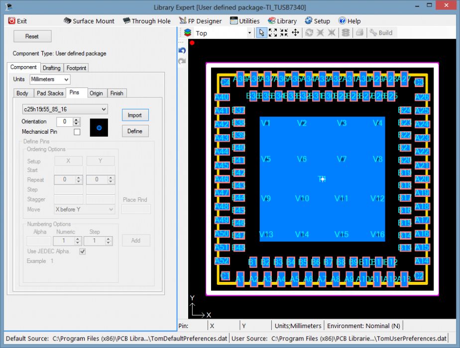
I would add vias in the PCB layout so you can move them around for routing inner layer traces or even remove some if they block routing. However, if you do want to add vias to the thermal tab in the footprint, you can easily do this in the FP Designer. I would create a .csv ASCII text file that looks like this and import it to add all the vias - V1 -2.45 2.45 V2 -0.87 2.45 V3 0.87 2.45 V4 2.45 2.45 V5 -2.45 0.87 V6 -0.87 0.87 V7 0.87 0.87 V8 2.45 0.87 V9 -2.45 -0.87 V10 -0.87 -0.87 V11 0.87 -0.87 V12 2.45 -0.87 V13 -2.45 -2.45 V14 -0.87 -2.45 V15 0.87 -2.45 V16 2.45 -2.45 You can import a text file with coordinates to insert any specific pad stack. |
|
 |
|
Tom H 
Admin Group 

Joined: 05 Jan 2012 Location: San Diego, CA Status: Offline Points: 6029 |
 Post Options Post Options
 Thanks(0) Thanks(0)
 Quote Quote  Reply Reply
 Posted: 25 Oct 2013 at 6:22am Posted: 25 Oct 2013 at 6:22am |
|
Here is a Dual Row QFN that I built in FP Designer and imported the text file to insert the vias -
 |
|
 |
|
michaelhallin 
New User 
Joined: 14 Jan 2013 Location: Denmark Status: Offline Points: 3 |
 Post Options Post Options
 Thanks(0) Thanks(0)
 Quote Quote  Reply Reply
 Posted: 25 Oct 2013 at 6:33am Posted: 25 Oct 2013 at 6:33am |
|
Thanks. The reason I want them in the footprint is that all my footprints also has paste mask defined, and I dont want paste in the vias. The paste mask pattern covers the via holes.
Are there any chance this will be implemented in the GUI?. |
|
 |
|
Tom H 
Admin Group 

Joined: 05 Jan 2012 Location: San Diego, CA Status: Offline Points: 6029 |
 Post Options Post Options
 Thanks(0) Thanks(0)
 Quote Quote  Reply Reply
 Posted: 25 Oct 2013 at 1:27pm Posted: 25 Oct 2013 at 1:27pm |
|
You can control the Thermal Pad Paste Mask % and you can turn that layer on to see the checkerboard pattern.
In FP Designer you can manually place the vias on a snap grid in-between the checkerboard patterns. Interactive Graphic Editing will come some time in V2014. |
|
 |
|
Mattylad 
Advanced User 
Joined: 02 Jun 2012 Location: Lancashire UK Status: Offline Points: 152 |
 Post Options Post Options
 Thanks(0) Thanks(0)
 Quote Quote  Reply Reply
 Posted: 06 Nov 2013 at 3:17pm Posted: 06 Nov 2013 at 3:17pm |
On the other hand, many others who lay out boards recognise that it is a very good suggestion to put them in the footprint itself. If you add vias per PCB then it is easy to accidentally unroute them, when you move the component the vias do not move with it, if you forget to add the vias even worse etc. So having the thermal vias in the centre of a heatsink pad as permanent features in a footprint that will always be there, not unrouted or forgotten can actually make the layout easier to do and trouble free. You should not remove them for routing - they are there for a purpose. Thank you for adding this in FPD now, but what are the values referenced to? Can you provide more information on how to do this? perhaps one of your nice videos? |
|
 |
|
Post Reply 
|
|
| Tweet |
| Forum Jump | Forum Permissions  You cannot post new topics in this forum You cannot reply to topics in this forum You cannot delete your posts in this forum You cannot edit your posts in this forum You cannot create polls in this forum You cannot vote in polls in this forum |