

|
|
Solder Mask Oversize? |
Post Reply 
|
| Author | |
Kenji 
Active User 
Joined: 23 May 2016 Status: Offline Points: 35 |
 Post Options Post Options
") Thanks(0) Thanks(0)
 Quote Reply Quote Reply
 Topic: Solder Mask Oversize? Topic: Solder Mask Oversize?Posted: 03 Sep 2017 at 10:32pm |
|
I usually use FP Designer. Then I have a question regarding the corner chamfer. The component picture has the solder mask oversize 0.05 mm equally. 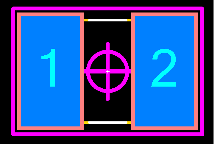 I edited the pad stack to use the chamfer feature. But but how do you make the solder mask oversize 0.05 mm equally? 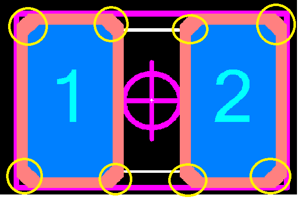 |
|
 |
|
|
|
|
Tom H
Admin Group 

Joined: 05 Jan 2012 Location: San Diego, CA Status: Offline Points: 5716 |
Post Options
Thanks(0)
Quote Reply
Posted: 04 Sep 2017 at 6:09am |
|
In FP Designer you can edit the full pad stack (Top, Solder Mask and Paste Mask" in "Pad Stack Manager".
Select the layer you want to edit and change the values for both the Top and Solder Mask separately. Note: the solder mask chamfer will be slightly larger than the Top pad. Let us know if you need a webcast training session and we'll set it up immediately. |
|
|
|
|
Kenji
Active User
Joined: 23 May 2016 Status: Offline Points: 35 |
Post Options
Thanks(0)
Quote Reply
Posted: 04 Sep 2017 at 5:44pm |
|
I knew. I use the pad stack manager. But The program has only a Chamfer's length.
All I want to do is to have a gap between Top and Solder Mask Top.
|
|
|
|
|
Tom H
Admin Group
Joined: 05 Jan 2012 Location: San Diego, CA Status: Offline Points: 5716 |
Post Options
Thanks(0)
Quote Reply
Posted: 04 Sep 2017 at 6:01pm |
|
Unfortunately, you have to figure out the solder mask chamfer size for the solder mask layer.
0.05 mm pad chamfer = 0.075 mm solder mask chamfer to keep the 0.05 mm oversize. Or you can create a new pad stack in the "Pad Stack Designer" with a 0.05 mm solder mask over size and it will auto-calculate a new pad stack. Then swap out the pin numbers with the new pad stack in the "Pad Stack Manager". |
|
|
|
|
Kenji
Active User
Joined: 23 May 2016 Status: Offline Points: 35 |
Post Options
Thanks(0)
Quote Reply
Posted: 04 Sep 2017 at 6:59pm |
|
Thanks.
0.05 mm pad chamfer = 0.075 mm solder mask chamfer to keep the 0.05 mm oversize. This is good idea. The other idea about creating a new pad stack in Pad Stack Designer is unsatisfactory, because It creates a 0.10 mm solder mask chamfer and the annular area is narrower than 0.05 mm.
|
|
|
|
|
Tom H
Admin Group
Joined: 05 Jan 2012 Location: San Diego, CA Status: Offline Points: 5716 |
Post Options
Thanks(0)
Quote Reply
Posted: 07 Sep 2017 at 9:34am |
|
We fixed this FP Designer Chamfered Pad Solder Mask issue and re-released V2017.17.
Try the updated version. |
|
|
|
|
NoellEagan
New User 
Joined: 19 Oct 2017 Status: Offline Points: 1 |
Post Options
Thanks(0)
Quote Reply
Posted: 19 Oct 2017 at 9:54am |
|
Hi,
I am a new user here. As per my knowledge in FP Designer you can edit the full pad stack (Top, Solder Mask and Paste Mask) in "Pad Stack Manager". Also you should select the layer you want to edit and change the values for both the Top and Solder Mask separately. |
|
|
|
|
Post Reply
|
|
| Tweet |
| Forum Jump | Forum Permissions You cannot post new topics in this forum You cannot reply to topics in this forum You cannot delete your posts in this forum You cannot edit your posts in this forum You cannot create polls in this forum You cannot vote in polls in this forum |


 Topic Options