SON / QFN Calculations
Printed From: PCB Libraries Forum
Category: PCB Footprint Expert
Forum Name: Questions & Answers
Forum Description: issues and technical support
URL: https://www.PCBLibraries.com/forum/forum_posts.asp?TID=889
Printed Date: 01 Jun 2026 at 5:37am
Topic: SON / QFN Calculations
Posted By: jnelso09
Subject: SON / QFN Calculations
Date Posted: 15 Mar 2013 at 5:55am
|
The algorithm for calculating the center (thermal) land dimensions for QFN/SON is fundamentally flawed. Why? Because it assumes maximum tolerance dimensions for the center land and then trims the inside of the peripheral lands to achieve the desired gap around the center pad. This will almost always create a land pattern that is non-symmetric with respect to the component pads. Because QFN's are fabricated from sheet copper in an array, the tolerance of the pads vary uniformly (for the most part) with respect to the etch process. This means that if the center pad is over-etched then the outer pads are also over-etched. And if the center pad is under-etched then so are the outer pads. Furthermore, the component peripheral pad length is also dictated by a saw or punch tolerance which has nothing to do with the etch tolerance and therefore should be considered independently AFTER the etch tolerances are accounted for. This is why is makes more sense to apply a uniform 'trimming' to both the center land and the inside of the peripheral lands - it maintains symmetry with the component fabrication etch process. My suggestion is to change the algorithm to calculate the center land dimensions based upon the nominal centerline of the gap around the component center pad. To calculate the center land dimensions use the nominal values for: Component package width (A), Thermal pad width (Wt), Peripheral land length (T), Pullback (PB), and center pad gap (g). The center land dimension equals (A+Wt)/2 - T - PB - g. If this number is larger than the maximum tolerance value of the center pad (Wtmax) then use Wtmax instead.
For a detailed discussion of this topic please reference my whitepaper:
http://smta.org/knowledge/journal_detail.cfm?ARTICLE_ID=208" rel="nofollow - BOTTOM TERMINATION COMPONENT LAND PATTERN DESIGN AND ASSEMBLY http://smta.org/knowledge/journal_detail.cfm?ARTICLE_ID=208" rel="nofollow -
http://smta.org/knowledge/journal_detail.cfm?ARTICLE_ID=208" rel="nofollow - FOR HIGH RELIABILITY ELECTRONIC SYSTEMS
|
Replies:
Posted By: Tom H
Date Posted: 15 Mar 2013 at 7:16am
|
My suggestion is to use the component mfr. recommended thermal pad size using the "Footprint Tab". The mfr. does testing for thermal cycle, shock and vibration on their recommended patterns and I've come to trust them, as I've never had a problem yet when I follow their recommendations. |
Posted By: jnelso09
Date Posted: 15 Mar 2013 at 12:47pm
|
Our experience has been that vendor recommended footprints for QFN devices either don't exist or they are contrary to applications for high-reliability hardware. For instance, we have found several vendors that recommend a solder mask defined center pad. We have found that when the center pad is completely surrounded by solder mask voiding in the solder joint increases and the ability to clean flux residues out from under these parts is difficult if not impossible. Of course this is coming from the high-rel mentality so commercial users would not be exposed to or even care about these issues. Below is a micro-section of a typical SON device that failed test for certain RF performance characteristics. We were never able to conclude the root cause but it was believed to be due to center pad voiding and/or flux trapped around the perimeter of the center pad. 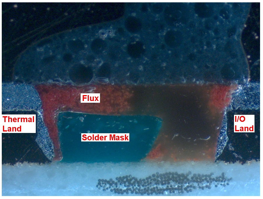 |
Posted By: jnelso09
Date Posted: 15 Mar 2013 at 1:31pm
This might also help to clarify . . .
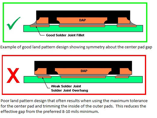 |
Posted By: jnelso09
Date Posted: 15 Mar 2013 at 1:34pm
| Ooops! I just noticed that the previously posted pic shows exactly the opposite of what I'm talking about - The center land is minimized and the outer lands are maximized. Same idea though - just switch the center pad to maximum tolerance and trim the outer lands. |