Free Footprint Calculator or Footprint Expert?
Printed From: PCB Libraries Forum
Category: PCB Footprint Expert
Forum Name: Features & Training
Forum Description: quick-start tips, images, videos, training, and webinars
URL: https://www.PCBLibraries.com/forum/forum_posts.asp?TID=3466
Printed Date: 21 Jul 2026 at 6:37am
Topic: Free Footprint Calculator or Footprint Expert?
Posted By: Nick B
Subject: Free Footprint Calculator or Footprint Expert?
Date Posted: 24 Jan 2025 at 11:03pm
|
The free Footprint Calculator and the Footprint Expert are compared here: https://www.pcblibraries.com/products/compare" rel="nofollow - https://www.pcblibraries.com/products/compare To download and use the free Footprint Calculator: 1. Login at https://www.PCBLibraries.com/downloads" rel="nofollow - https://www.PCBLibraries.com/downloads (login with existing account, or register for free) 2. If you see this button, click it: 3. If you do not see it, you already have a Key. Click this button to download: 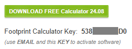 4. Install and run the Calculator, then use your Email and Key (full key displayed on Download page) to activate the Calculator license.  PCB Footprint Expert To get a fully functional Footprint Expert license, complete the Evaluation License request on the Downloads page. Make sure to provide all the requested information, such as your company details and CAD outputs needed. Get your FREE Footprint Calculator or Footprint Expert Evaluation License: https://www.pcblibraries.com/Register" rel="nofollow - https://www.PCBLibraries.com/Register Call: 847-557-2300 ------------- Stay connected - follow us! https://twitter.com/PCBLibraries" rel="nofollow - X - http://www.linkedin.com/company/pcb-libraries-inc-/" rel="nofollow - LinkedIn |
Replies:
Posted By: Nick B
Date Posted: 30 Jan 2025 at 12:12pm
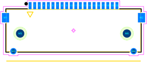
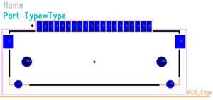
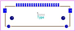
The details below are just some of the differences (yes, there are more!) between the Footprint Expert footprints and the libraries available all over the internet. Most don’t realize how lacking all those footprints online really are, but they can be much worse than lacking when they actually cost you money.
The Footprint Expert automates footprints to perfection. Professional, detailed, and accurate parts – all built consistently with identical rules, regardless of how many people are involved in your library development. Get your FREE Footprint Calculator or Footprint Expert Evaluation License: https://www.pcblibraries.com/Register" rel="nofollow - https://www.PCBLibraries.com/Register Call us - 847-557-2300 ------------- Stay connected - follow us! https://twitter.com/PCBLibraries" rel="nofollow - X - http://www.linkedin.com/company/pcb-libraries-inc-/" rel="nofollow - LinkedIn |
||||||||||||||||||||||||||||||||||||||||||||||||