Placement Courtyard Excess
Printed From: PCB Libraries Forum
Category: Libraries
Forum Name: PCB Library Construction Guidelines
Forum Description: Documentation of the Footprint Expert Guidelines
URL: https://www.PCBLibraries.com/forum/forum_posts.asp?TID=3372
Printed Date: 27 Jul 2026 at 12:53pm
Topic: Placement Courtyard Excess
Posted By: Tom H
Subject: Placement Courtyard Excess
Date Posted: 07 Apr 2024 at 2:54pm
|
IPC-7351B refers to a 0.25 Courtyard Excess for Nominal Density Level. However, feedback from our customers indicate 0.20 Courtyard Excess works perfect. The Least Density Courtyard Excess is 0.10, Nominal 0.20 and Most is 0.40. There are 2 courtyard settings. One for the package body and one for the pads. The Package Body uses the Maximum package dimension. Some Enterprise CAD tools turn the courtyard excess off to contour the courtyard to the maximum package dimensions. Then they use the courtyard for Placement Boundary or use the CAD tool rules for footprint to footprint spacing rules. The manufacturing zone is intended for assembly shops who need more area around the footprint pattern. Your assembly shop needs to communicate this information.  ------------- Stay connected - follow us! https://twitter.com/PCBLibraries" rel="nofollow - X - http://www.linkedin.com/company/pcb-libraries-inc-/" rel="nofollow - LinkedIn |
Replies:
Posted By: achico
Date Posted: 20 Feb 2025 at 5:34am
From IPC-7352 I found this information, is it correct? It seems to be different as to IPC-7351B referenced.
|
| 0.50 mm | 1.00 mm | ||
| 0.25 mm | 0.50 mm | ||
| 0.20 mm | 0.25 mm | ||
| 0.75 mm | 1.25 mm | ||
| 0.50 mm | 1.00 mm | ||
| 0.25 mm | 0.50 mm |
Posted By: Tom H
Date Posted: 20 Feb 2025 at 9:14am
|
IPC-7352 does not break down the courtyard to Pad and Body separately. The solder joint goal tables only refer to one courtyard Excess.
However, PCB Libraries customers think the Least value of 0.10 is OK, but then they double that for Nominal to 0.20 and then double that for Most to 0.40. Also, Siemens, Cadence and Zuken users turn off all Courtyard Excess values and use the courtyard as a placement boundary outline and they use internal CAD tool spacing rules for part placement. Both the Nominal and Most Density Levels pass all Class 3 stress tests for shock and vibration, thermal cycling and drop tests. So the Most Density is rarely used in production. But some mil spec contractors still use the Most Density Level, even though the Nominal Density Level performance is equal. But the Courtyard Excess values are user definable so some companies might use the Most pad stack calculation and a Nominal Courtyard Excess. The main point is that many PCB designers think outside the box and use IPC-7352 as a "Guideline" but don't use it verbatim. They glean some information from IPC but develop internal standards that work best with their assembly process. Another thing that many people don't understand is that IPC only offers guidelines for pad stacks and courtyard and don't have much information on all the elements that go into a footprint pattern. Here is an example of some things IPC does not provide guidelines and details for a typical land pattern: 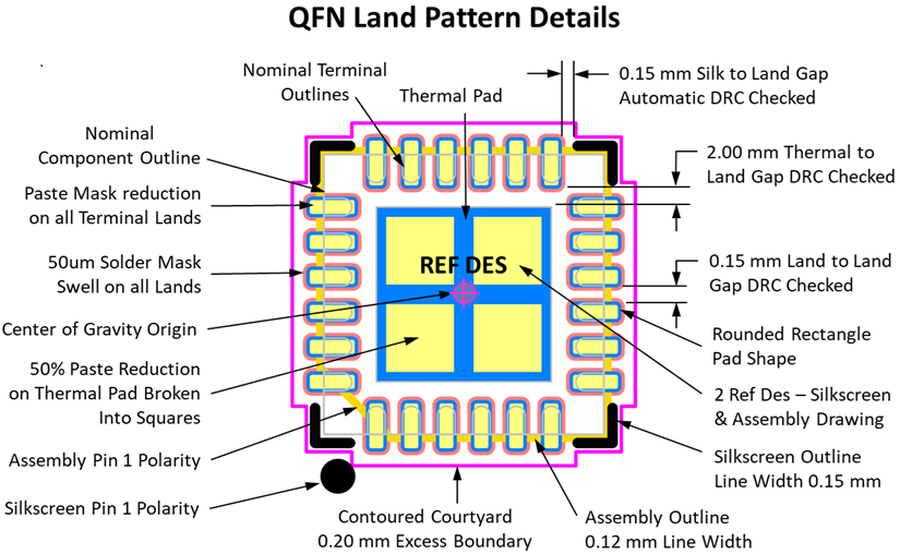 ------------- Stay connected - follow us! https://twitter.com/PCBLibraries" rel="nofollow - X - http://www.linkedin.com/company/pcb-libraries-inc-/" rel="nofollow - LinkedIn |
Posted By: achico
Date Posted: 21 Feb 2025 at 12:27am
|
Thank you Tom for your clarifications and realistic industry point of view, much appreciated. Best regards |