Who is IPC and How Do They Affect PCB Libraries?
Printed From: PCB Libraries Forum
Category: Libraries
Forum Name: Footprints / Land Patterns
Forum Description: [General or a CAD specific issues / discussions]
URL: https://www.PCBLibraries.com/forum/forum_posts.asp?TID=2584
Printed Date: 29 Apr 2026 at 10:25am
Topic: Who is IPC and How Do They Affect PCB Libraries?
Posted By: Tom H
Subject: Who is IPC and How Do They Affect PCB Libraries?
Date Posted: 18 Dec 2019 at 2:26pm
|
The organization started in 1957 by 6 PCB manufacturers as the Institute for Printed Circuits.
In 1977 IPC changed its name to the
Association Connecting Electronics Industries after multiple assembly manufacturers
started getting involved. In 1999, the organization formally revised its name
to IPC “Association Connecting Electronics Industries”. IPC is the only trade association that brings together all of the
players in the electronics industry: PCB designers, board manufacturers,
assembly companies, suppliers, and original equipment manufacturers. When all
of these industry leaders work together, we can develop standards that make
everyone more productive by reducing errors and increasing quality. This
ultimately leads to faster time to market for all companies. However, not all
companies follow IPC standards. They have their own internal technical
development talent for the sole purpose of making their electronic product
development automation successful. IPC has its
headquarters in Bannockburn, Ill., and has other offices around the United
States and the world, including in India, China, Sweden and Russia. IPC boasts of more than 5,400 companies around the world that
depend on IPC programs and services to further their competitive excellence and
financial success. There are over 3,600 IPC certified trainers worldwide to
train and test on the two major standards, IPC-A-610 for PCB fabrication and
IPC-J-STD-001 for PCB assembly. There are
more than 110 IPC licensed training centers around the world. The organization
also offers online and multimedia educational and training resources. It hosts
educational events, as well as technical and management conferences including
IPC APEX EXPO, which is the largest electronics manufacturing industry
exhibition in North America, and APEX South China.
IPC-A-610 is used by every Fabrication shop in the electronics industry
to manufacture PCB’s for their customers end-use, which are broken up into 3
Classes, 1, 2 or 3. CLASS 1 – General Electronic Products Includes products suitable for applications where the major requirement is function of the completed assembly. Least expensive manufacturing cost. Toys CLASS 2 –
Dedicated Service Electronic Products Includes products where continued performance and extended life is
required, and for which uninterrupted service is desired but not critical.
Typically, the end-use environment would not cause failures. Nominal expensive
manufacturing cost. Computers & Phones CLASS 3 –
High Performance Electronic Products Includes products where continued high performance or
performance-on-demand is critical, equipment downtime cannot be tolerated,
end-use environment may be uncommonly harsh, and the equipment must function
when required, such as life support or other critical systems. Most expensive
manufacturing cost. Military & Medical IPC-J-STD-001 defines the requirements for electronic assemblies. Land pattern footprint pad sizes and locations play a significant role in meeting these requirements.
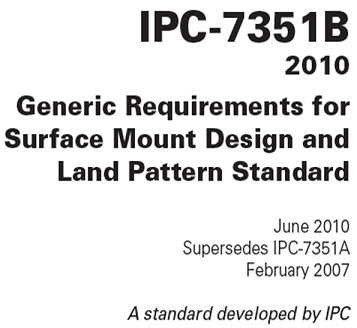
The IPC-7351 guideline falls under IPC-J-STD-001 to define the solder joint goals for Toe, Heel and Side values and the land pattern and pad stack naming conventions. The land pattern footprint pad size is determined by the terminal
lead size, the terminal lead tolerances, the manufacturing tolerances for
fabrication and assembly and the Toe, Heel and Side solder joint goals as
defined in the IPC-7351 guideline.
This combination of features and tolerances is commonly referred to as “The IPC-7351 Mathematical Model for Land Pattern Calculation”. ------------- Stay connected - follow us! https://twitter.com/PCBLibraries" rel="nofollow - X - http://www.linkedin.com/company/pcb-libraries-inc-/" rel="nofollow - LinkedIn |


