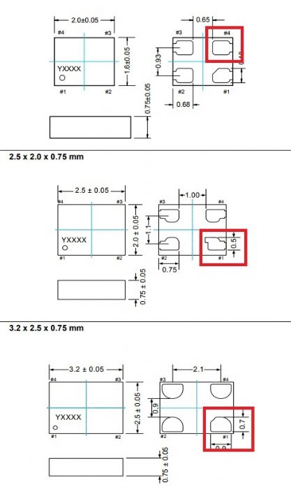
How To Draw Footprint for the Attached Case?
Printed From: PCB Libraries Forum
Category: General
Forum Name: General Discussion
Forum Description: general topics not related to other forums
URL: https://www.PCBLibraries.com/forum/forum_posts.asp?TID=2182
Printed Date: 12 May 2026 at 7:55am
Topic: How To Draw Footprint for the Attached Case?
Posted By: Hassan Moaaz
Subject: How To Draw Footprint for the Attached Case?
Date Posted: 04 Jul 2017 at 6:13am
How can i draw foot print for cases like in below image |
Replies:
Posted By: Tom H
Date Posted: 04 Jul 2017 at 7:40am
|
Right now you have to purchase credits and we will build it for you. We're adding interactive graphic editing in the new V2019 Library Expert. ------------- Stay connected - follow us! https://twitter.com/PCBLibraries" rel="nofollow - X - http://www.linkedin.com/company/pcb-libraries-inc-/" rel="nofollow - LinkedIn |
Posted By: CloseCl
Date Posted: 25 Aug 2017 at 4:53am
That's really good news. |
Posted By: Tom H
Date Posted: 25 Aug 2017 at 7:43am
|
However, the component manufacturer recommends a rectangle pad pattern for these parts. ------------- Stay connected - follow us! https://twitter.com/PCBLibraries" rel="nofollow - X - http://www.linkedin.com/company/pcb-libraries-inc-/" rel="nofollow - LinkedIn |
 Tom H wrote: