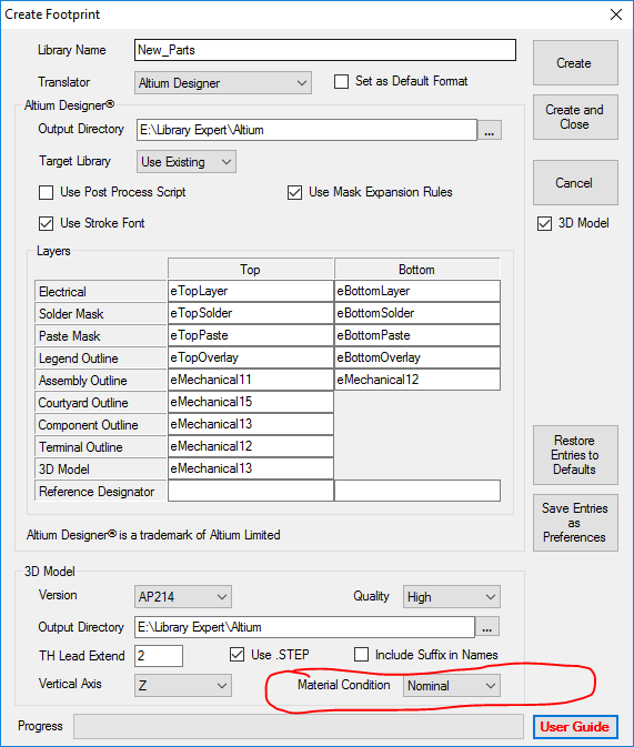
"Material Condition" for 3D model
Printed From: PCB Libraries Forum
Category: PCB Footprint Expert
Forum Name: Questions & Answers
Forum Description: issues and technical support
URL: https://www.PCBLibraries.com/forum/forum_posts.asp?TID=2051
Printed Date: 26 Jul 2026 at 3:11pm
Topic: "Material Condition" for 3D model
Posted By: ransonjd
Subject: "Material Condition" for 3D model
Date Posted: 05 Jan 2017 at 2:49pm
|
What does the "Material Condition" drop down change when building 3D models for a component? --JOhn
|
Replies:
Posted By: Tom H
Date Posted: 05 Jan 2017 at 3:01pm
|
In the Calculator dimensional panel the user either inputs the Nominal & Tolerance or the Minimum and Maximum package values. If you insert Nominal and Tolerance. the dimensional panel auto-fills the Min & Max dimensions. If you insert the Min & Max dimensions the dimensional panel auto-fills the Nominal and Tolerance values. Either way, Minimum, Nominal and Maximum dimensions are always there. When creating the 3D STEP model the Material Condition setting will use the dimensional data in whatever column it's set to. i.e.: if you select Maximum Material Condition then the 3D STEP model uses the Maximum package dimensions to create the model. Note: you can insert 100 million different component package dimensions and auto-generate 100 million 3D STEP models. I say this because some users do not realize that every 3D model is 100% customized per the package dimensions in the Land Pattern Calculator. ------------- Stay connected - follow us! https://twitter.com/PCBLibraries" rel="nofollow - X - http://www.linkedin.com/company/pcb-libraries-inc-/" rel="nofollow - LinkedIn |
Posted By: ransonjd
Date Posted: 05 Jan 2017 at 5:12pm
|
Okay, that's what I suspected. It seemed like it wasn't working, but I just realized that the part was created in FP Designer and the body is not toleranced. --John
|
Posted By: Tom H
Date Posted: 05 Jan 2017 at 5:56pm
|
I should have put emphases on "Calculator" parts with all package dimensions and not Non-standard mfr. recommended patterns (FP Designer). ------------- Stay connected - follow us! https://twitter.com/PCBLibraries" rel="nofollow - X - http://www.linkedin.com/company/pcb-libraries-inc-/" rel="nofollow - LinkedIn |