How To Genereate CAPAE Footprint?
Printed From: PCB Libraries Forum
Category: PCB Footprint Expert
Forum Name: Questions & Answers
Forum Description: issues and technical support
URL: https://www.PCBLibraries.com/forum/forum_posts.asp?TID=1957
Printed Date: 06 Jun 2026 at 9:24pm
Topic: How To Genereate CAPAE Footprint?
Posted By: Sujith
Subject: How To Genereate CAPAE Footprint?
Date Posted: 12 Sep 2016 at 6:23am
|
Hi, I am new to this tool. I was trying to generate a footprint foor SMD Aluminium Capacitorm but no success ! 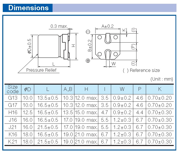  whats wrong am doing? please help
|
Replies:
Posted By: Tom H
Date Posted: 12 Sep 2016 at 7:09am
|
Do you see the blue dots in the dimensions? Only enter any 2 of 3 that you want and never enter all 3. You'll get bad results due to over calculation of tolerances. ------------- Stay connected - follow us! https://twitter.com/PCBLibraries" rel="nofollow - X - http://www.linkedin.com/company/pcb-libraries-inc-/" rel="nofollow - LinkedIn |
Posted By: Sujith
Date Posted: 12 Sep 2016 at 8:43am
|
Ahh..yes, I missed it. It got worked now..  . .In the component data sheet by the mafr the pads values are : L=5.5, W=1.2+-0.3, P=6.7 . is this values are based on nominal or most or least? and the generated footprints measurement were : Most Nominal Least L=6.83 L=6.46 L=6.12 W=2.7 W=2.52 W=2.31 other dimensions like outline and courtyards also varies, i didt checked. here I got the width of the pads entirely wrong it seems? and its a bit confusing which footprint (n,m,l) to use , in the internet most people suggests to use nominal footprints. Actually what is the best practice to follow?
|
Posted By: Tom H
Date Posted: 12 Sep 2016 at 9:08am
|
Most people use Nominal Density Level, which is a default setting. Maximum Density is used for space satellites. Least Density Level is used for RF design or extremely dense designs. ------------- Stay connected - follow us! https://twitter.com/PCBLibraries" rel="nofollow - X - http://www.linkedin.com/company/pcb-libraries-inc-/" rel="nofollow - LinkedIn |
Posted By: Sujith
Date Posted: 12 Sep 2016 at 9:36pm
|
Ok...thanks for the info. but how to get the correct pad width? instead of 1.2 +-0.3 am getting 2.51
|
Posted By: Tom H
Date Posted: 13 Sep 2016 at 7:38am
|
The solder joint goals in LE Lite are in the tab Terminal > Density Level > Toe, Heel and Side. You can control the entire solder joint by adjusting those values. ------------- Stay connected - follow us! https://twitter.com/PCBLibraries" rel="nofollow - X - http://www.linkedin.com/company/pcb-libraries-inc-/" rel="nofollow - LinkedIn |