SMD (Solder Mask Defined) and NSMD Pads
Printed From: PCB Libraries Forum
Category: PCB Footprint Expert
Forum Name: Questions & Answers
Forum Description: issues and technical support
URL: https://www.PCBLibraries.com/forum/forum_posts.asp?TID=1768
Printed Date: 27 Jun 2026 at 2:46am
Topic: SMD (Solder Mask Defined) and NSMD Pads
Posted By: drj-bbe
Subject: SMD (Solder Mask Defined) and NSMD Pads
Date Posted: 24 Sep 2015 at 5:45pm
|
Hi Tom:
I know BGA land pattern design have two method, SMD(solder mask defined) and NSMD (non-solder-mask-defined), NSMD will be good than SMD for BGA pad to increase solder joint reliability. What about other components? chip, sop, connector and etc. Is NSMD also priority option for most components? Is there any related description in IPC/JEDEC standard? |
Replies:
Posted By: Tom H
Date Posted: 24 Sep 2015 at 9:36pm
|
BGA pad size and solder joint relation is totally different than Chip, SOP and Connectors. The NSMD BGA pad stack is necessary for the Ball to fully collapse around the pad edge securing it to the PCB - 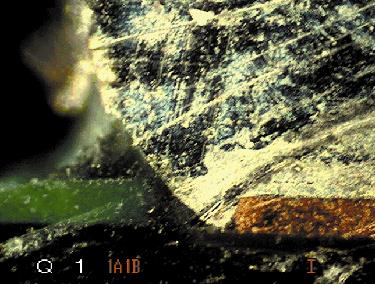 The SMD (Solder Mask Defined) BGA pad stack prevents the Ball Collapse - 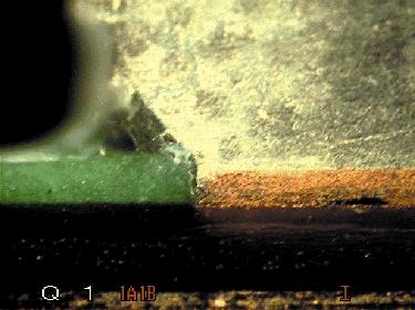 The BGA ball melts during reflow and other component leads do not. ------------- Stay connected - follow us! https://twitter.com/PCBLibraries" rel="nofollow - X - http://www.linkedin.com/company/pcb-libraries-inc-/" rel="nofollow - LinkedIn |
Posted By: drj-bbe
Date Posted: 24 Sep 2015 at 10:26pm
|
So, which method will be better for PCB land pattern soldered BGA? I have seen a describtion in IPC-7093 6.1.3.6 solder mask design. NSMD is better than SMD on QFN solder joint strenth. Should I assume that NSMD is first option for other chip, sop and connectors.
What about your opinion?
|
Posted By: Tom H
Date Posted: 25 Sep 2015 at 5:20am
|
NSMD is normally used on every SMT pad due to registration tolerance of +/- 0.05 mm. You do not want any solder mask on the pad so the minimum solder mask opening should be 0.05 mm. The exception to this rule is Flexible Circuit libraries normally have a 0.05 mm solder mask over the Toe and Heel of the pad to act as an epoxy glue to hold the pad down while flexing the board. ------------- Stay connected - follow us! https://twitter.com/PCBLibraries" rel="nofollow - X - http://www.linkedin.com/company/pcb-libraries-inc-/" rel="nofollow - LinkedIn |