Pin1 / Package marking
Printed From: PCB Libraries Forum
Category: PCB Footprint Expert
Forum Name: Questions & Answers
Forum Description: issues and technical support
URL: https://www.PCBLibraries.com/forum/forum_posts.asp?TID=1667
Printed Date: 12 Jun 2026 at 11:33am
Topic: Pin1 / Package marking
Posted By: Luke
Subject: Pin1 / Package marking
Date Posted: 06 May 2015 at 11:16pm
|
Hello. I have a package that has the markings on pin 4 and NOT pin 1. Is there a way to change "pin 1" to another pin, say 4? Regards, Luke 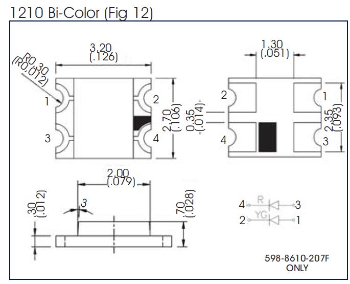 |
Replies:
Posted By: Tom H
Date Posted: 07 May 2015 at 9:12am
|
You should be using the "Side Concave Package (2, 4 pins) component family. You can select any Pin and RMB > Reorder pins. But it looks like the default pin assignment matches the default calculator pin assignment. 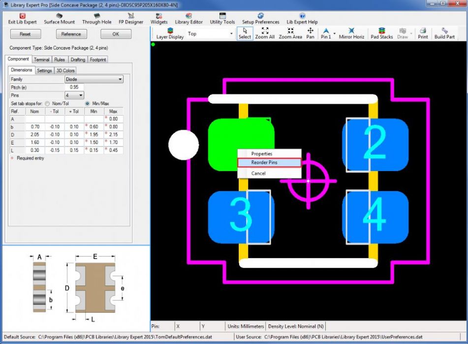 ------------- Stay connected - follow us! https://twitter.com/PCBLibraries" rel="nofollow - X - http://www.linkedin.com/company/pcb-libraries-inc-/" rel="nofollow - LinkedIn |