Make All Silkscreen Outlines The Same Format
Printed From: PCB Libraries Forum
Category: PCB Footprint Expert
Forum Name: Product Suggestions
Forum Description: request new features
URL: https://www.PCBLibraries.com/forum/forum_posts.asp?TID=1643
Printed Date: 13 Jul 2026 at 6:15pm
Topic: Make All Silkscreen Outlines The Same Format
Posted By: JJonas
Subject: Make All Silkscreen Outlines The Same Format
Date Posted: 11 Apr 2015 at 4:31am
|
I have reported an issue with silkscreen outline being drawn incorrectly some time ago and Tom has reported back that this bug was fixed. I have downloaded the latest version (2015.10) and I see that it is not fixed. Your tool is doing as shown in the first picture, while it should do as shown in the second picture. You can try it with Vertical Header or just about any other THD part. 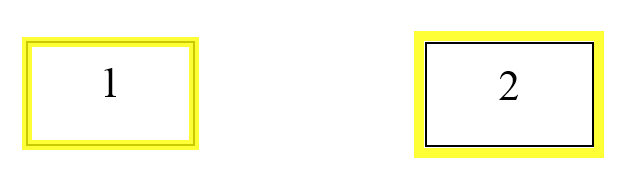
One more thing - why do you keep deleting Bug Reports that are solved? I have never seen such a practice in any other forum. Usually, when bug is fixed user or moderator marks that topic with a tag [SOLVED]. For example, in this case I had to recreate this bug report, because moderator has already deleted it.
|
Replies:
Posted By: Tom H
Date Posted: 11 Apr 2015 at 6:46am
|
The silkscreen boundary can map to the Minimum, Nominal or Maximum component outline. The system default is the Maximum component outline but the user can change it to whatever they want in Default Preferences > Drafting > Silkscreen > Map Silkscreen Outline to Body. The Yellow line represents the Maximum component outline. The Green outline represents the Nominal component outline. The White outlines represent the Maximum component outline and as you can see the inside border of the silkscreen maps to the Maximum Outline. The silkscreen outline is 100% outside the Maximum component body size. 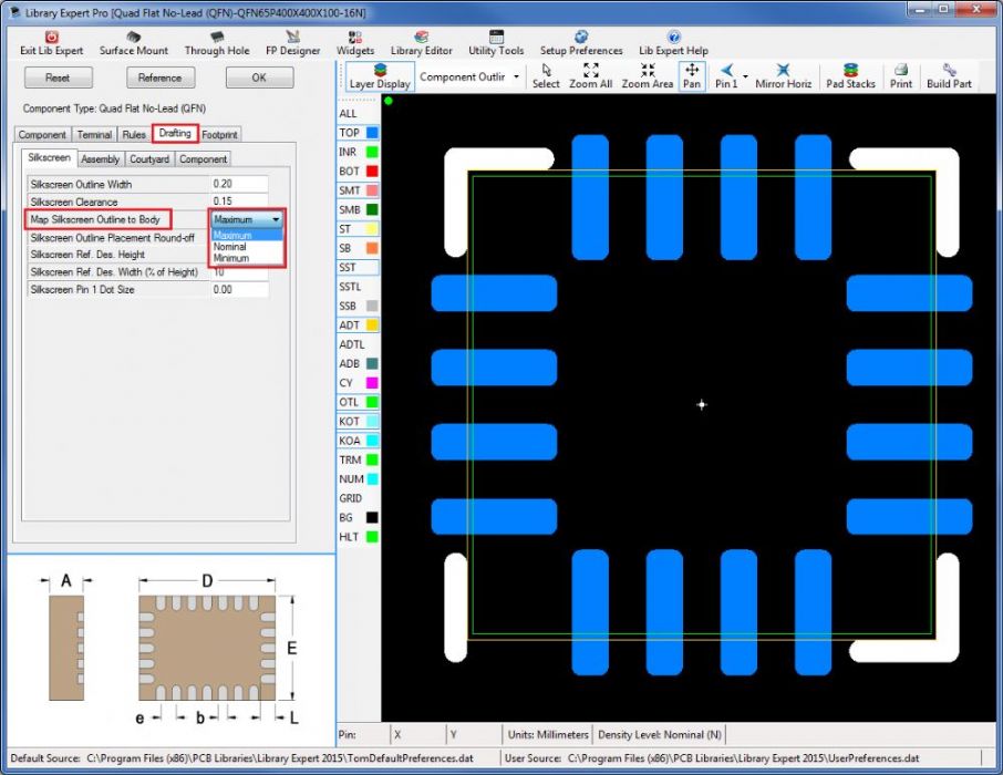 When a Library Expert user posts in the Bug Report Forum and the topic is not really a bug, they are removed as soon as possible. If the bug topic has any educational content relocated into the Q & A forum. No real bug report ever gets deleted, it gets recorded in the Version History located here - http://www.pcblibraries.com/forum/version-history_forum1.html" rel="nofollow - http://www.pcblibraries.com/forum/version-history_forum1.html The Bug Forum is strictly used by our customers to report issues and our programming staff to respond to users that they can replicate the bug and that they have resolved the issue in a version pre-release that is ready to be tested. Once the new software version is released, all bug fixes going back to the first release in July 2012 are posted forever in the Version History Forum and they are removed from the Bug Forum unless the bug is unresolved (then it will remain here until it's fixed or addressed). We like to release software with "all known bugs fixed" and normally do not release software with a known bug in it. ------------- Stay connected - follow us! https://twitter.com/PCBLibraries" rel="nofollow - X - http://www.linkedin.com/company/pcb-libraries-inc-/" rel="nofollow - LinkedIn |
Posted By: JJonas
Date Posted: 11 Apr 2015 at 2:37pm
Tom, you are trying it with SMD components. I have suggested using THD parts, for example, Vertical Header. If you try it, you will see that the following will not be the case - "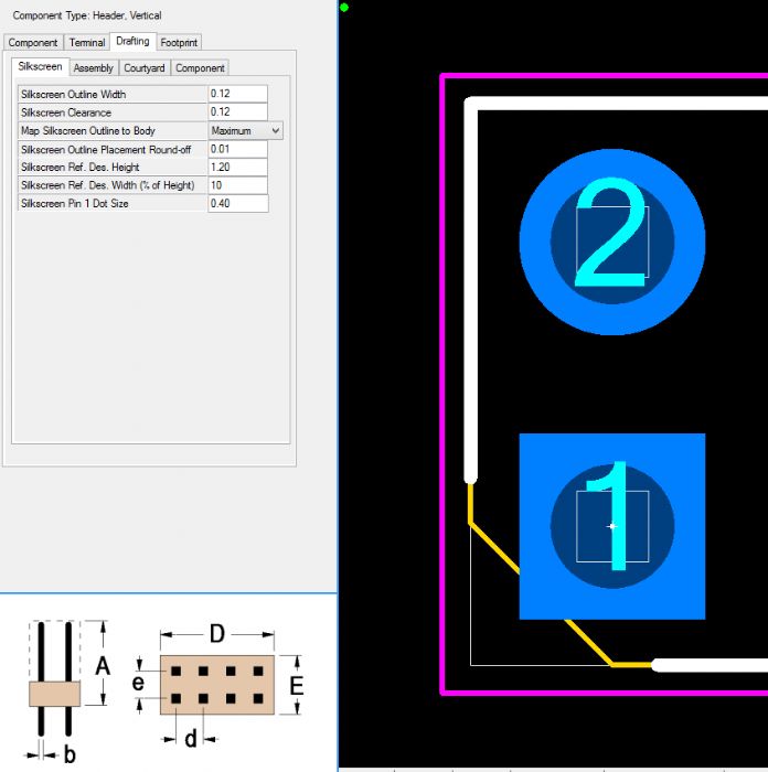 |
Posted By: Jeff.M
Date Posted: 14 Apr 2015 at 8:23pm
|
Please note that for all PTH types only a Maximum body dimension is accepted. Without going going into why this is the case, it is impossible for now to map any PTH part to other than a maximum dimension. A change to this practice is in the works. ------------- Stay connected - follow us! https://twitter.com/PCBLibraries" rel="nofollow - X - http://www.linkedin.com/company/pcb-libraries-inc-/" rel="nofollow - LinkedIn |
Posted By: JJonas
Date Posted: 29 Apr 2015 at 11:04am
| Tom, V11 is released, but this issue is still not fixed as promised. |
Posted By: Tom H
Date Posted: 29 Apr 2015 at 11:14am
|
You are correct. Right now we are focusing on some major new feature updates and do not have the time to backtrack and fix something that has been in the program since July 2012. We think our time is better spent of creating some spectacular new features that will be released on June 1st. However, we do eventually plan on backtracking and fixing the Through-hole silkscreen outlines so they map the same as the SMD outlines. But the timeframe is unclear. I would like to announce that we will be rewriting from scratch Library Expert for 2016 as we need to add many new features that our customers have been asking for over the years but the existing software program was limited to be able to add them. So I can promise that all the silkscreen outlines will match the same rules in V2016.01 due out later this year. ------------- Stay connected - follow us! https://twitter.com/PCBLibraries" rel="nofollow - X - http://www.linkedin.com/company/pcb-libraries-inc-/" rel="nofollow - LinkedIn |
Posted By: JJonas
Date Posted: 29 Apr 2015 at 12:54pm
|
To tell you the truth, that is a disappointing answer to hear. A software package that is supposed helping engineers to follow defined standards is not doing its prime job. You say that this bug is present from mid-2012. This means that users of this software package were building and using inconsistent footprints and most likely did not suspect that. A natural question arises – why would anyone should continue using your software package if they need to manual fix inaccuracies and inconsistencies produced by your software package? I am confident that an average user does not care about new features, new GUI etc. if basic features are not working or if they are working incorrectly. I strongly believe that developers of a software package that is supposed to enforce accuracy, consistency and compliance with standards should focus on fixing bugs instead of spending time redesigning GUI. In other words, accuracy first and new features later. By the way, you have once again deleted my reported bug (silkscreen not being within a courtyard) without fixing it. I am not going to report it again. |
Posted By: Tom H
Date Posted: 01 May 2015 at 7:55am
|
This issue is not an easy fix, but we will get to it when we have time. Also, all Resolved or Duplicate forum posts are Archived (not deleted). ------------- Stay connected - follow us! https://twitter.com/PCBLibraries" rel="nofollow - X - http://www.linkedin.com/company/pcb-libraries-inc-/" rel="nofollow - LinkedIn |
Posted By: Tom H
Date Posted: 03 Aug 2015 at 6:48pm
|
We just added Receptacle and Shrouded Vertical Headers with high quality 3D STEP in V2015.16 that will be available tomorrow. ------------- Stay connected - follow us! https://twitter.com/PCBLibraries" rel="nofollow - X - http://www.linkedin.com/company/pcb-libraries-inc-/" rel="nofollow - LinkedIn |