Option to Enable/Disable Pin One Silk and Assy
Printed From: PCB Libraries Forum
Category: PCB Footprint Expert
Forum Name: Questions & Answers
Forum Description: issues and technical support
URL: https://www.PCBLibraries.com/forum/forum_posts.asp?TID=1548
Printed Date: 16 Mar 2026 at 8:42pm
Topic: Option to Enable/Disable Pin One Silk and Assy
Posted By: josanche
Subject: Option to Enable/Disable Pin One Silk and Assy
Date Posted: 06 Feb 2015 at 10:02am
|
Hi, is there any chance we can have the option to enable/disable the assembly outline chamfer? My company doesn't utilize this, so each time I have to delete the assy outline within the cell editor (expedition) and recreate without. Quite inefficient :( 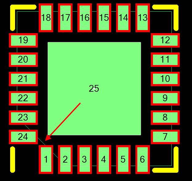 As well as the silkscreen outline pin one indicator (in this case the removal of a line from the silk outline)? I always have to re-create the silkscreen in that corner fix this, and it would be nice if I had to option to turn it off so it would leave the silk intact identical to the other three corners. 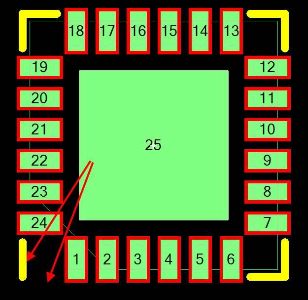 |
Replies:
Posted By: Tom H
Date Posted: 06 Feb 2015 at 10:10am
|
You can download the latest V2015.08 pre-release here - http://www.pcblibraries.com/downloads" rel="nofollow - www.pcblibraries.com/downloads New feature that allows you to output the component body and terminal leads separately. Instead of using the Assembly Outline, use the Component Outline (no polarity). You can adjust the line width and the layer assignment. As far as the Silkscreen Outline, there are new standard guidelines that prohibit the silkscreen to be outside the courtyard or under the component package. For "Bottom Only Terminal" components, the absence of silkscreen is the polarity marker. What do you do to fix the Polarity Marker?
------------- Stay connected - follow us! https://twitter.com/PCBLibraries" rel="nofollow - X - http://www.linkedin.com/company/pcb-libraries-inc-/" rel="nofollow - LinkedIn |
Posted By: josanche
Date Posted: 09 Feb 2015 at 9:24am
|
Does the "Component Outline" exist in expedition? And if so what is it called? I used it in Library expert per your example and there is nothing that imported for me on the mentor side. We love the program and would love it even more if some of these functions had the ability to be toggled on or off. Thanks!!!!
|
Posted By: Tom H
Date Posted: 10 Feb 2015 at 9:21am
|
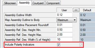
OK, in V2015.08 we have 3 new toggle preferences - Available later today Drafting > Assembly > Polarity Indicator, new button to toggle the assembly outline polarity chamfer
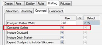
Drafting > Courtyard > Contour Courtyards, new button to toggle between Contour and Rectangle courtyards
Drafting > Silkscreen > Polarity Indicator, new button to toggle the silkscreen outline polarity chamfer ------------- Stay connected - follow us! https://twitter.com/PCBLibraries" rel="nofollow - X - http://www.linkedin.com/company/pcb-libraries-inc-/" rel="nofollow - LinkedIn |