Footprint for Molded Body
Printed From: PCB Libraries Forum
Category: PCB Footprint Expert
Forum Name: Questions & Answers
Forum Description: issues and technical support
URL: https://www.PCBLibraries.com/forum/forum_posts.asp?TID=1396
Printed Date: 16 Jun 2026 at 11:54pm
Topic: Footprint for Molded Body
Posted By: JJonas
Subject: Footprint for Molded Body
Date Posted: 25 Aug 2014 at 5:32pm
I am not 100% sure, but it seems that footprint is not correctly generated for molded body packages. In my example, b and b1 is set to be max 1 mm, however, W and W1 is calculated to be only 0.93, why not >=1?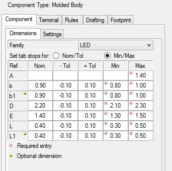 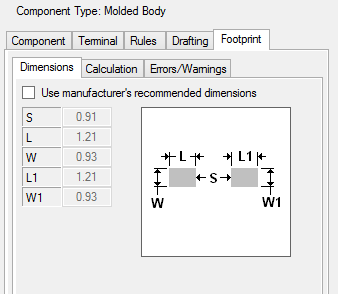 |
Replies:
Posted By: Tom H
Date Posted: 25 Aug 2014 at 6:57pm
|
The answer to your question is that the "Side" solder joint goals for the pad width calculation are equal to or less than the Max Lead Width. This is correct according to the IPC-7351 solder joint goal chart for the "Inward L-Bend" component lead. But you have access in the User Preferences to change that value. That's the beauty of the Professional version. Also, I would remove the redundant "b1" and "L1" component dimensions. They are strictly for when Pin 2 is a different size. If Pin 1 and 2 are identical there is no need for "b1" and "L1" component dimensions. Also, in the Footprint Tab if the component mfr. provides a recommended patter, I often enter those dimensions here and then see the Viewer for the component Lead on top of pad to visualize the solder joint. But there is the Calculation Tab that provides all the Toe, Heel and Side Min. & Max. goals. ------------- Stay connected - follow us! https://twitter.com/PCBLibraries" rel="nofollow - X - http://www.linkedin.com/company/pcb-libraries-inc-/" rel="nofollow - LinkedIn |