Silkscreen for connectors
Printed From: PCB Libraries Forum
Category: PCB Footprint Expert
Forum Name: Questions & Answers
Forum Description: issues and technical support
URL: https://www.PCBLibraries.com/forum/forum_posts.asp?TID=1394
Printed Date: 14 May 2026 at 9:46am
Topic: Silkscreen for connectors
Posted By: JJonas
Subject: Silkscreen for connectors
Date Posted: 24 Aug 2014 at 10:11am
|
Can anyone advice me how should silkscreen look like for connectors? For example this one: 
How should I identify the first pin (or corner where that pin is located)?
|
Replies:
Posted By: Tom H
Date Posted: 24 Aug 2014 at 11:30am
|
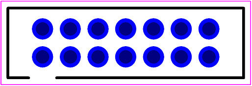
Sometimes the absence of silkscreen makes the best polarity marker. But you need to make the silkscreen outline so that it's visible after assembly. Reason: Adding silkscreen text or triangles or dots usually hinders part placement on high density boards. It's OK to add pin number text if your PCB layouts are low density, but that does not seem to be the common case anymore. If you use placement courtyards, all silkscreen outlines should be located inside the courtyard. This picture has a courtyard (magenta) and a silkscreen outline. Can you immediately tell where Pin 1 is? Can the assembly shop tell where pin 1 is?
I would like constructive feedback on why this type of polarity marking is OK or not good. ------------- Stay connected - follow us! https://twitter.com/PCBLibraries" rel="nofollow - X - http://www.linkedin.com/company/pcb-libraries-inc-/" rel="nofollow - LinkedIn |
Posted By: Dale
Date Posted: 24 Aug 2014 at 4:22pm
|
The part in question looks like it would be hand placed. In that context I would argue that the primary use of the silkscreen is as an assembly aid, and therefore it should mimic/emphasise the obvious/non-obvious polarizing feature(s) of the part.
|
Posted By: Tom H
Date Posted: 24 Aug 2014 at 7:03pm
|
Yes, the silkscreen is a post-assembly inspection aid to assist the end-user to visually inspect that every component was not inversely inserted.
------------- Stay connected - follow us! https://twitter.com/PCBLibraries" rel="nofollow - X - http://www.linkedin.com/company/pcb-libraries-inc-/" rel="nofollow - LinkedIn |
Posted By: ernestorey
Date Posted: 25 Aug 2014 at 10:12am
| In my experience the most important function of the silkscreen for a connector is to illustrate whether it is mounted on the top or bottom side of the board. |
Posted By: JJonas
Date Posted: 25 Aug 2014 at 4:50pm
- Looking at your picture, yes, I can immediately tell where pin 1 is. I am not sure if it will be as obvious in real life because cutout is very small (~1 mm). And what if there is a slight offset (either of silkscreen or connector)?  - What if we use the same connector but in SMD package? Then we cannot place cutout of silkscreen directly at that pin. In addition, there is no much space between the first pin and the top of connector.  |
 Tom H wrote:
Posted By: Tom H
Date Posted: 25 Aug 2014 at 5:05pm
|
All very good points. I'm glad that we're having a discussion on silkscreen polarity marking because we're in search of the perfect solution to this issue. ------------- Stay connected - follow us! https://twitter.com/PCBLibraries" rel="nofollow - X - http://www.linkedin.com/company/pcb-libraries-inc-/" rel="nofollow - LinkedIn |
Posted By: jameshead
Date Posted: 26 Aug 2014 at 2:13am
|
I could work it out. This is a "grey area" because I specifically advise on my silkscreen layers that the silkscreen should not be used for component assembly - that's what the centroid x/y data and assembly drawing is for. I'm happy for pin 1 on the assembly drawing to be a dot or a triangle or chamfered corner, as long as it's noticeable. That said the silkcreen should still be useful as an aid for hand-insertion. Whether it's a dot or a line doesn't matter as long as there's a consistant style on the board and for a particular customer. Personally on some connectors I add silkcreen to resemble the connector in some way to make it clear. On a screw terminal block I add a solid block of silkscreen to indicate the back, solid end of the connector. On a wire to board connector with a friction lock such as the Molex 22-27-2xx1 series I will add solid silkscreen blocks for the friction lock. On an IDC shrouded header I will add a solid silkcreen block to indicate the polarising cut-out in the shroud where it doesn't interfere with the pads. If I can't do anything obvious and sensible then I will leave it to the assembly diagram to show it more clearly and add a line for pin 1. |