

|
|
Pad to Pad space in 3-pin SOFL |
Post Reply 
|
| Author | |
Batiskaff 
Advanced User 
Joined: 30 Apr 2018 Status: Offline Points: 65 |
 Post Options Post Options
") Thanks(0) Thanks(0)
 Quote Reply Quote Reply
 Topic: Pad to Pad space in 3-pin SOFL Topic: Pad to Pad space in 3-pin SOFLPosted: 03 Mar 2021 at 2:47am |
|
In Rules "Pad to Pad" spacing = 0.15mm But pads were trimmed and now Pad1 to Pad2 space=0.33mm 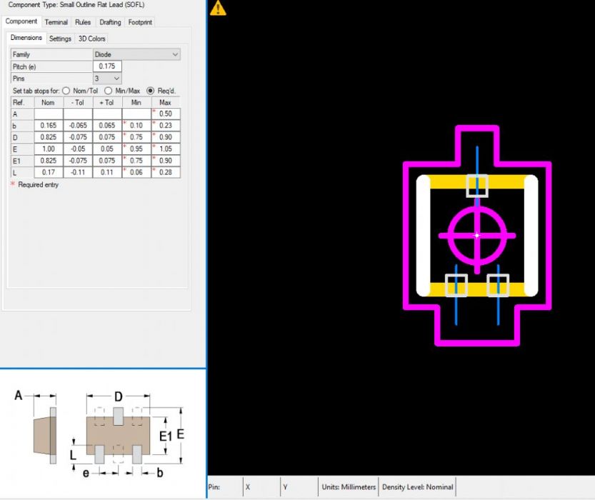 |
|
 |
|

|
|
|
|
|
Tom H
Admin Group 

Joined: 05 Jan 2012 Location: San Diego, CA Status: Offline Points: 5993 |
Post Options
Thanks(0)
Quote Reply
Posted: 03 Mar 2021 at 10:08am |
|
The Pad Stack Rules are intended for medium to large packages.
You can't have a pin pitch of 0.175 when the maximum lead thickness is 0.23. That's impossible. Turn the minimum pad to pad off for micro-miniature packages. The pin pitch is 0.175. This can't be true. The pin pitch is between the Center of the Body and the center of the pin. You need to double to pin pitch to 0.35 mm. But I would also change the solder joint goals downward slightly. Please provide a link to the datasheet URL. |
|
|
|
|
Batiskaff
Advanced User
Joined: 30 Apr 2018 Status: Offline Points: 65 |
Post Options
Thanks(0)
Quote Reply
Posted: 03 Mar 2021 at 11:53am |
|
|
|
Tom H
Admin Group
Joined: 05 Jan 2012 Location: San Diego, CA Status: Offline Points: 5993 |
Post Options
Thanks(0)
Quote Reply
Posted: 03 Mar 2021 at 12:13pm |
|
This package in not a SOTFL.
The SOTFL component family has the Terminal Lead Width the same size for all leads. This JEITA-SC-1168B case code is none standard and must use the mfr. recommended footprint. Package: 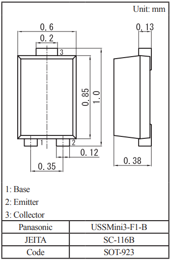 Mfr. Recommended footprint: 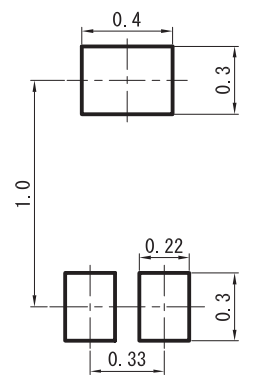 |
|
|
|
|
Post Reply
|
|
| Tweet |
| Forum Jump | Forum Permissions You cannot post new topics in this forum You cannot reply to topics in this forum You cannot delete your posts in this forum You cannot edit your posts in this forum You cannot create polls in this forum You cannot vote in polls in this forum |


 Topic Options