

|
|
OrCAD 17.2: END LAYER Regular Pad Is Undefined |
Post Reply 
|
Page 12> |
| Author | |
dmonca 
Advanced User 
Joined: 13 Dec 2012 Location: Switzerland Status: Offline Points: 59 |
 Post Options Post Options
") Thanks(1) Thanks(1)
 Quote Reply Quote Reply
 Topic: OrCAD 17.2: END LAYER Regular Pad Is Undefined Topic: OrCAD 17.2: END LAYER Regular Pad Is UndefinedPosted: 13 Sep 2016 at 6:28am |
|
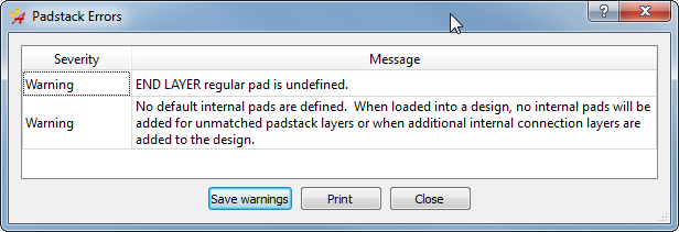
We recently updated our OrCAD PCB-Editor to 17.2. Now LE can not build TH footprints anymore. The new Padstack Editor always throws up this warning:
 This is the script that caused the error (just as an example, since all others behave the same way): # Allegro script # Generated by FPX Expert # name: s218h145 QtSignal MainWindow New triggered QtSignal fileNewDialog dataCombo CurrentIndexChanged "Thru Pin" QtSignal fileNewDialog dataCombo activated "Thru Pin" QtSignal fileNewDialog browse clicked QtFillin s218h145.pad QtSignal fileNewDialog OK clicked QtSignal MainWindow Units CurrentIndexChanged Millimeter QtFillin Yes QtSignal MainWindow DecimalPlaces activated 4 QtSignal GuidedDrillTab HoleType activated Circle QtSignal GuidedDrillTab holeXSize editingFinished 1.45 QtSignal GuidedDesignLayersTab LayersTable cellClicked 0 "Regular Pad" None 0 2 QtSignal GuidedDesignLayersTab PadShape CurrentIndexChanged Square QtSignal GuidedDesignLayersTab PadShape activated Square QtSignal GuidedDesignLayersTab PadWidth editingFinished 2.18 QtSignal GuidedDesignLayersTab LayersTable cellClicked 1 "Regular Pad" None 1 2 QtSignal GuidedDesignLayersTab PadShape CurrentIndexChanged Circle QtSignal GuidedDesignLayersTab PadShape activated Circle QtSignal GuidedDesignLayersTab PadDiameter editingFinished 2.18 QtSignal GuidedDesignLayersTab LayersTable cellClicked 1 "Thermal Pad" None 1 3 QtSignal GuidedDesignLayersTab PadShape CurrentIndexChanged Circle QtSignal GuidedDesignLayersTab PadShape activated Circle QtSignal GuidedDesignLayersTab PadDiameter editingFinished 2.3 QtSignal GuidedDesignLayersTab LayersTable cellClicked 1 "Anti Pad" None 1 4 QtSignal GuidedDesignLayersTab PadShape CurrentIndexChanged Circle QtSignal GuidedDesignLayersTab PadShape activated Circle QtSignal GuidedDesignLayersTab PadDiameter editingFinished 2.3 QtSignal GuidedDesignLayersTab LayersTable cellClicked 2 "Regular Pad" None 2 2 QtSignal GuidedDesignLayersTab PadShape CurrentIndexChanged Square QtSignal GuidedDesignLayersTab PadShape activated Square QtSignal GuidedDesignLayersTab PadWidth editingFinished 2.18 QtSignal GuidedMaskLayersTab LayersTable cellClicked 0 Pad None 0 1 QtSignal GuidedMaskLayersTab PadShape CurrentIndexChanged Square QtSignal GuidedMaskLayersTab PadShape activated Square QtSignal GuidedMaskLayersTab PadWidth editingFinished 2.18 QtSignal GuidedMaskLayersTab LayersTable cellClicked 1 Pad None 1 1 QtSignal GuidedMaskLayersTab PadShape CurrentIndexChanged Square QtSignal GuidedMaskLayersTab PadShape activated Square QtSignal GuidedMaskLayersTab PadWidth editingFinished 2.18 QtSignal GuidedDrillSymbol FigureType CurrentIndexChanged Cross QtSignal GuidedDrillSymbol FigureType activated Cross QtSignal GuidedDrillSymbol FigureWidth editingFinished 1.0 QtSignal GuidedDrillSymbol FigureHeight editingFinished 1.0 QtSignal MainWindow Save triggered QtSignal MainWindow Exit triggered I have already checked the psmpath and psmpath settings and the both conatin the "." in the first place (although I don't think that this is the problem here, sinc SM Parts build correctly). I am running LE2016.10 Any ideas how to fix this? Regards Daniel |
|
 |
|

|
|
|
|
|
tbest
New User 
Joined: 28 Oct 2015 Status: Offline Points: 6 |
Post Options
Thanks(1)
Quote Reply
Posted: 13 Sep 2016 at 7:34am |
|
I've just encountered this issue as well. I deleted the last two lines in the script, which allowed me to see all the parameters the script is editing.
Currently, the script is only populating the "Regular Pad" column on the "Begin Layer" row under the "Design Layers" tab. Pad Editor isn't making the padstack because it doesn't have enough info to do so. The same thing is occurring on the "Mask Layers" tab, but I don't think that affects the error we're seeing. Might just have to manually add the information in Pad Editor for now.
|
|
|
|
|
chrisa_pcb
Moderator Group 

Joined: 29 Jul 2012 Location: San Diego Status: Offline Points: 772 |
Post Options
Thanks(0)
Quote Reply
Posted: 13 Sep 2016 at 10:19am |
|
Out of curiousity.. do you still have 16.6 loaded? 16.6 uses pad_designer, whereas 17.2 uses the new padstack_editor. I've had issues with 16.6 also being on my machine when trying to run 17.2. Make sure you use the Cadence Switch Release program to set the release to 17.2. As a check, I just ran thru-hole reference parts with both square and circle pads without issue, and they mirror what you have above, so I don't think its a problem with the script. I think its getting its wires crossed trying to run the 17.2 programs. Here is what the new padstack_editor looks like: 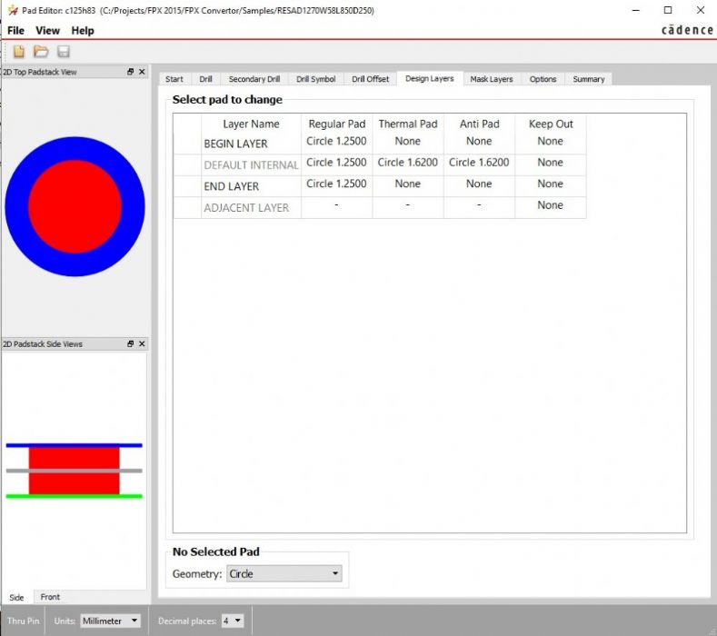 |
|
|
|
|
dmonca
Advanced User
Joined: 13 Dec 2012 Location: Switzerland Status: Offline Points: 59 |
Post Options
Thanks(0)
Quote Reply
Posted: 14 Sep 2016 at 12:07am |
|
Hi Chris Nope. Version 16.6 is not installed. I removed it after installing the new release. As best mentioned: Also on my machine, only the beginning layer gets its information from the script. The rest of the fields stay empty (set to "none") |
|
|
|
|
chrisa_pcb
Moderator Group
Joined: 29 Jul 2012 Location: San Diego Status: Offline Points: 772 |
Post Options
Thanks(0)
Quote Reply
Posted: 14 Sep 2016 at 9:54am |
|
Try running the script manually using the file -> script command and see what happens.
|
|
|
|
|
dmonca
Advanced User
Joined: 13 Dec 2012 Location: Switzerland Status: Offline Points: 59 |
Post Options
Thanks(0)
Quote Reply
Posted: 15 Sep 2016 at 11:11pm |
|
Hi Chris
Unfortunately still the same behaviour. |
|
|
|
|
chrisa_pcb
Moderator Group
Joined: 29 Jul 2012 Location: San Diego Status: Offline Points: 772 |
Post Options
Thanks(0)
Quote Reply
Posted: 16 Sep 2016 at 11:13am |
|
Actually... can you send me the part in FPX form? Or at the least screenshot your dimensions so I can replicate? Lets see if I can get that part to throw the error. I'll send you my email by PM. Lets talk there so we can get this worked out.
|
|
|
|
|
BennsPCB
Advanced User
Joined: 30 Jan 2013 Location: Sweden Status: Offline Points: 98 |
Post Options
Thanks(0)
Quote Reply
Posted: 19 Sep 2016 at 4:45am |
|
When I start the padstack_editor stand-alone, it starts in my HOME-directory instead of what I would prefer the PSMPATH-directory.
I also reported another issue concerning the missing searchpath to the binarys for "padstack_editor" and "allegro", i.e no footprint creation at all. Cadence does not set them anymore in 17.2 /my 5 cents |
|
|
|
|
jrosal
New User
Joined: 10 Dec 2012 Status: Offline Points: 6 |
Post Options
Thanks(1)
Quote Reply
Posted: 21 Sep 2016 at 12:41pm |
|
I'm also getting this "End layer undefined" and "No Internal Layers Defined" warning when trying to generate through hole footprints. Surface mount footprints works fine.
I'm also using 2016.10. |
|
|
|
|
chrisa_pcb
Moderator Group
Joined: 29 Jul 2012 Location: San Diego Status: Offline Points: 772 |
Post Options
Thanks(0)
Quote Reply
Posted: 21 Sep 2016 at 1:52pm |
|
Ok. I got this covered with jrosal. Here is the fix. It should be in the new pre-release tomorrow and .11 should be hitting next week. · Allegro/OrCAD PCB – Between builds S002 and S005, Cadence slightly modified the syntax of one of the commands used by the 17.2 scripting. A change has been made to reflect this, but it will BREAK all builds before S005. You *must* upgrade to S005 or later of Allegro/OrCAD PCB after you implement this patch. This will also fix the No DEFAULT INTERNAL issue that people on S005 were having. |
|
|
|
|
Post Reply
|
Page 12> |
| Tweet |
| Forum Jump | Forum Permissions You cannot post new topics in this forum You cannot reply to topics in this forum You cannot delete your posts in this forum You cannot edit your posts in this forum You cannot create polls in this forum You cannot vote in polls in this forum |


 Topic Options