
 |

|
No Option For Pad Round-off In V2021 Edition? |
Post Reply 
|
Page <123> |
| Author | |
Tom H 
Admin Group 

Joined: 05 Jan 2012 Location: San Diego, CA Status: Online Points: 5993 |
 Post Options Post Options
 Thanks(0) Thanks(0)
 Quote Quote  Reply Reply
 Posted: 09 Apr 2021 at 8:36am Posted: 09 Apr 2021 at 8:36am |
|
The Land Pattern Naming Convention must have 3 places because of the way it was designed and created.
XX.XX for the values. 2 places to the left of the decimal point and 2 places to the right of the decimal point. I guess you didn't understand 2 X 2 Decimal Place Accuracy like you set in the Console Options. Was this the problem that wasn't really a problem? When you select Decimal Place Accuracy to 2 min and 3 max, it still produces the same footprint name because that is the standard naming convention. i.e.: you can't change the naming convention regardless of your Decimal Place Accuracy because the naming convention is a standard XX.XX for now according to IPC-7351. Note: all leading zero's "0" are dropped and ending zero's are not. |
|
 |
|

|
|
 |
|
Quist 
New User 
Joined: 21 Jun 2018 Status: Offline Points: 3 |
 Post Options Post Options
 Thanks(0) Thanks(0)
 Quote Quote  Reply Reply
 Posted: 09 Apr 2021 at 11:07am Posted: 09 Apr 2021 at 11:07am |
|
Ah, no I was not referring to the Naming Convention but rather to the actual pad dimensions presented under Footprint -> Manufacturer's Dimensions.
I got the impression that no matter what decimal accuracy I put in I got three decimal places on the dimensions but now I can't reproduce the behaviour so it was probably user induced... I see in our fpx library that we have a different number of decimal places on the pads for different components. That might have been whats fooled me. Can you please comment on the subtitle "Manufacturer's Dimensions". Who is Manufacturer referring to, component manufacturer or PCB manufacturer? I find it a bit confusing. Wouldn't it be better to call it something like "Pad dimensions" and the checkbox something like "Use custom dimensions" or similar? |
|
 |
|
Tom H 
Admin Group 

Joined: 05 Jan 2012 Location: San Diego, CA Status: Online Points: 5993 |
 Post Options Post Options
 Thanks(0) Thanks(0)
 Quote Quote  Reply Reply
 Posted: 09 Apr 2021 at 11:42am Posted: 09 Apr 2021 at 11:42am |
|
The Manufacturer reference is the Component Manufacturer, not the fabrication or assembly shops.
The current pad stack and footprint naming conventions are intentionally created in 0.01 mm increments because if you added one more place to accommodate 0.001 accuracy, the footprint name would be too long for most CAD tools. Right now, the character limit for a footprint name is 40 characters. If you added one more number to each value the footprint name would be 47+ characters. Body Length X Width X Height X Lead Width X Length X Thermal Tab Width X Length Same with Pad Stack names. |
|
 |
|
Quist 
New User 
Joined: 21 Jun 2018 Status: Offline Points: 3 |
 Post Options Post Options
 Thanks(0) Thanks(0)
 Quote Quote  Reply Reply
 Posted: 09 Apr 2021 at 12:34pm Posted: 09 Apr 2021 at 12:34pm |
|
I agree, 0.01 mm is good for naming no matter what the physical accuracy is. I even seriously doubt that there is any practical benefit with going below 0.01 accuracy. Normal trace tolerance in an etch proces is probably around 0.05 mm and might be tweaked down to 0.02 mm.
Regarding "Manufacturer's Dimension": If I open a part in Footprint Expert and would like to see the size of the pads calculated by Footprint Expert the only way I know to do it is to go to the "Manufacturers Dimensions" section and look there. However, this is not the manufacturers dimensions but rather the dimensions calculated by Footprint Expert. I don't think the naming is intuitive. |
|
 |
|
Tom H 
Admin Group 

Joined: 05 Jan 2012 Location: San Diego, CA Status: Online Points: 5993 |
 Post Options Post Options
 Thanks(0) Thanks(0)
 Quote Quote  Reply Reply
 Posted: 09 Apr 2021 at 1:20pm Posted: 09 Apr 2021 at 1:20pm |
|
The pad stack naming convention used in Footprint Expert is available for free download on www.pcblibraries.com/downloads
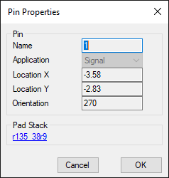
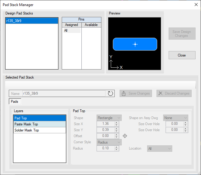
In Footprint Expert you can double click (or single click + RMB > Properties) any pad and the program will open the pad Properties.  If you select the Pas Stack name, it will open the Pad Stack Manager.  The values are grayed out for any Calculator footprint because if you edit it, PCB Libraries, Inc. or IPC cannot be responsible for any typos. But you can visually see the pad length and width and corner radius too. I can look at any pad stack name and tell you the length, width and corner radius. You can control the corner radius in Options > Pad Stack Rules > SMD Corner Rounding > Corner Size Limit The default is 0.25 but many users change that value to 0.10 or 0.05. |
|
 |
|
arendhagedoorn2 
New User 
Joined: 16 May 2015 Status: Offline Points: 3 |
 Post Options Post Options
 Thanks(0) Thanks(0)
 Quote Quote  Reply Reply
 Posted: 16 May 2021 at 11:24pm Posted: 16 May 2021 at 11:24pm |
|
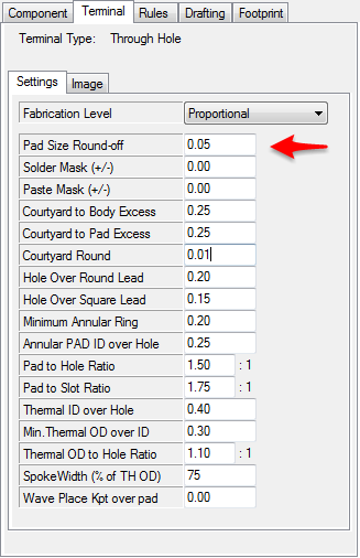
Hi Tom, I've read all the posts about this issue but
there is not realy a solution for the now missing pad round off. Is it
not possible to implement the pad round off just like it was in the
previous versions?:  Thank you and best regards, Arend
|
|
 |
|
Tom H 
Admin Group 

Joined: 05 Jan 2012 Location: San Diego, CA Status: Online Points: 5993 |
 Post Options Post Options
 Thanks(0) Thanks(0)
 Quote Quote  Reply Reply
 Posted: 17 May 2021 at 12:25pm Posted: 17 May 2021 at 12:25pm |
|
We're taking a look at adding the Plated Through-hole pad size round-off in V2021.05 this week.
The default value will be set to 0.01 but you can change it to whatever value you want. Thanks for the input. |
|
 |
|
Jeromeli 
Active User 
Joined: 10 Jun 2021 Status: Offline Points: 12 |
 Post Options Post Options
 Thanks(0) Thanks(0)
 Quote Quote  Reply Reply
 Posted: 16 Jun 2021 at 10:42pm Posted: 16 Jun 2021 at 10:42pm |
|
So is there a solution to this problem? Maybe we need to wait for a higher version?
|
|
 |
|
Tom H 
Admin Group 

Joined: 05 Jan 2012 Location: San Diego, CA Status: Online Points: 5993 |
 Post Options Post Options
 Thanks(0) Thanks(0)
 Quote Quote  Reply Reply
 Posted: 17 Jun 2021 at 8:18am Posted: 17 Jun 2021 at 8:18am |
|
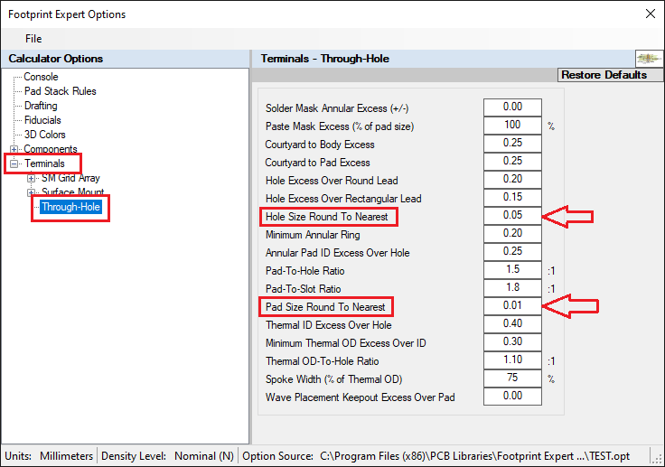
We added through-hole pad and hole size roundoff feature in V2021.08.
Look in Tools > Options > Terminals > Through-hole Change the values to whatever you want.  |
|
 |
|
Tom H 
Admin Group 

Joined: 05 Jan 2012 Location: San Diego, CA Status: Online Points: 5993 |
 Post Options Post Options
 Thanks(0) Thanks(0)
 Quote Quote  Reply Reply
 Posted: 02 Mar 2022 at 11:36am Posted: 02 Mar 2022 at 11:36am |
|
The latest V2022.03 release has a new Options feature for Pad Size Rounding.
2 = 0.01 round-off 3 = 0.001 round-off If you want a 0.05 round-off, select and open the Footprint panel and select "Use mfr. recommended pattern" and change the pad size to whatever you want. This process only takes 30 seconds. Note: IPC has no guidance on SMD pad size rounding. So, when you apply a 0.05 mm SMD pad size round-off, it's not IPC compliant per the 3-Tier Density Levels defined in the IPC-7351 guideline. Using a SMD pad Size Round-off of 0.05 mm cannot be classified as an IPC compliant pattern. The Pad Stack Naming Convention is in 0.01 mm increments. |
|
 |
|
Post Reply 
|
Page <123> |
| Tweet |
| Forum Jump | Forum Permissions  You cannot post new topics in this forum You cannot reply to topics in this forum You cannot delete your posts in this forum You cannot edit your posts in this forum You cannot create polls in this forum You cannot vote in polls in this forum |