|
|
Chip Component Package Tolerances |
Post Reply 
|
| Author | |
Tom H 
Admin Group 

Joined: 05 Jan 2012 Location: San Diego, CA Status: Offline Points: 6055 |
 Post Options Post Options
") Thanks(1) Thanks(1)
 Quote Reply Quote Reply
 Topic: Chip Component Package Tolerances Topic: Chip Component Package TolerancesPosted: 7 hours 6 minutes ago at 4:52pm |
|
Every aspect of a PCB mounted component has tolerances.
These include tolerances for Package length/width and terminals. The IPC-7351B refers to a
mathematical model that also includes fabrication and assembly tolerances.
IPC-7352 removed the manufacturing tolerances from the mathematical model. The mathematical model takes into consideration the minimum
and maximum package dimensions to ensure that the resulting land pattern
accommodates the package tolerance range. Tolerances are referred to as Min/Max
technology meaning the pad stack size and spacing regardless of if the
component package comes in the minimum or maximum material condition. Since the package and terminal tolerances affect the
resulting pad stack size and spacing, robust tolerances will produce larger pad
stacks while no tolerances will produce pad stacks that are too small. The IPC-7351
Side solder joint goal for chip packages is zero. The pad width is the same
dimension as the Maximum terminal lead width. The Heel solder joint goal for chip packages is zero. The
heel is determined by the terminal lead and package length tolerances. The Toe normally has a solder joint goal has a predefined
value. Then the terminal lead and package length tolerances are added to the
Toe value. The resulting Toe solder joint is a combination of the Toe goal
value and terminal and package length tolerances. Here are the recommended tolerances for the various chip
case codes:
Different component manufacturers will publish a wide range
of tolerances. For example, Panasonic, Yageo, Vishay, AVX, Murata, Kemet and
Taiyo Yuden will have different tolerances to the same Case Code. But the PCB
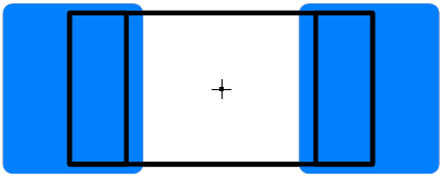
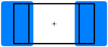
designer or CAD librarian want one set of tolerances for each Case Code. Here is a 0603 Chip with no tolerances:
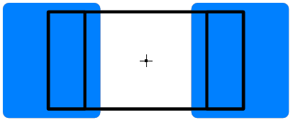
Here is a 0603 Chip with a 0.05 tolerance on Length, Width and Terminal Nominal Density Level:
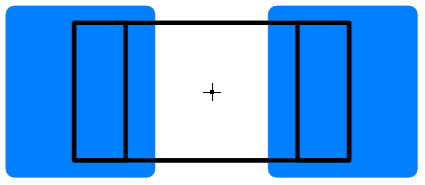
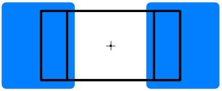
Here is a 0603 Chip with a 0.10 tolerance on Length, Width and Terminal Nominal Density Level:
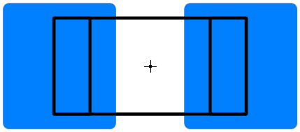
Here is a 0603 Chip with a 0.15 tolerance on Length, Width and Terminal Nominal Density Level:
Here is a 0603 Chip with a 0.20 tolerance on Length, Width and Terminal Nominal Density Level:
Here is a 0603 Chip with a 0.25 tolerance on Length, Width
and Terminal Nominal Density Level:
Here is a 0603 Chip with a 0.10 tolerance on Length, Width and Terminal Least Density Level:
Here is a 0603 Chip with a 0.10 tolerance on Length, Width and Terminal Most Density Level:
Chip component manufacturers do not use their package tolerances when publishing their manufacturer recommended patterns. They use nominal package dimensions and add a toe, heel and side solder joint regardless of how robust their tolerances are. If component tolerances are real and component packages can be shipped to assembly shops and some come in the minimum material condition and some come in the maximum material condition, there will be assembly attachment issues.  PCB Footprint Expert Simplify your PCB design process with the Footprint Expert, the ultimate tool - it can automatically rebuild entire libraries with modified tolerances. Automation helps ensures accurate, consistent, reliable footprints with minimal introduction of human error. Let the Footprint Expert handle your CAD library so you can focus on creating flawless PCB designs faster and more efficiently! Get your FREE Footprint Calculator or Footprint Expert Evaluation License: Call: 847-557-2300 |
|
 |
|

|
|
|
|
|
Post Reply
|
|
| Tweet |
| Forum Jump | Forum Permissions You cannot post new topics in this forum You cannot reply to topics in this forum You cannot delete your posts in this forum You cannot edit your posts in this forum You cannot create polls in this forum You cannot vote in polls in this forum |


 Topic Options