

|
|
Intended Stencil Thickness per IPC Standards |
Post Reply 
|
| Author | |
rweber 
New User 
Joined: 19 Feb 2025 Status: Offline Points: 2 |
 Post Options Post Options
") Thanks(0) Thanks(0)
 Quote Reply Quote Reply
 Topic: Intended Stencil Thickness per IPC Standards Topic: Intended Stencil Thickness per IPC StandardsPosted: 20 Feb 2025 at 11:28am |
|
Using the IPC standards used by Footprint Expert, is there an intended stencil thickness being considered? Stencil thickness is relevant since it is a factor in the volume of paste deposited, and the aperture area ratio/aspect ratio affecting paste release. For example, I often see example stencil designs on Texas Instruments datasheets that are given for a 0.125mm stencil thickness. |
|
 |
|
|
|
|
Tom H
Admin Group 

Joined: 05 Jan 2012 Location: San Diego, CA Status: Offline Points: 5761 |
Post Options
Thanks(0)
Quote Reply
Posted: 20 Feb 2025 at 4:50pm |
|
0.125 mm is a standard paste mask stencil thickness.
But microminiature footprints might have the stencil thinned to 0.10 mm. IPC-7525C Stencil Design Guidelines is the leading document. Rounded Rectangle apertures help stencil release for lead-free solder alloys. 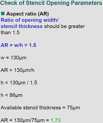 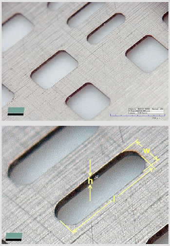 |
|
|
|
|
Post Reply
|
|
| Tweet |
| Forum Jump | Forum Permissions You cannot post new topics in this forum You cannot reply to topics in this forum You cannot delete your posts in this forum You cannot edit your posts in this forum You cannot create polls in this forum You cannot vote in polls in this forum |


 Topic Options