

 |

|
PCB Libraries Rounded Rectangle Pad Shape |
Post Reply 
|
| Author | |
Nick B 
Admin Group 
Joined: 02 Jan 2012 Status: Offline Points: 1925 |
 Post Options Post Options
 Thanks(0) Thanks(0)
 Quote Quote  Reply Reply
 Topic: PCB Libraries Rounded Rectangle Pad Shape Topic: PCB Libraries Rounded Rectangle Pad ShapePosted: 09 Jan 2025 at 8:23pm |
|
Popular Surface Mount footprint solder pattern shapes:
The rectangle pad shape was the first to be introduced in the 1980s primarily due to the limitation of the Gerber aperture wheel. PCB designers were forced to use 24 different aperture sizes in the Gerber format RS-274-D. This included every feature in the PCB layout. A trace width only required one aperture because it was an open shutter, dragged the aperture while open and close the shutter to complete. 1980s Gerber Aperture Wheel: 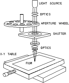 Back in the 1980s, PCB designers needed guidelines for surface mount PCB library creation. Jim Blankenhorn was one of the first to release the publication "SMT Plus" which was a huge success in providing dimensional data for the creation of CAD library footprints. Jim also offered land pattern training and education in the mid 1980s. The SMT Plus publication recommended rectangle pad shape. In the 1960s, 1970s and early 1980s, most PCB layouts were 100% through-hole. There weren’t any guidelines for Surface Mount technology and PCB designers needed guidelines for PCB library creation. IPC-SM-782 "Surface Mount Design and Land Pattern Standard" was released in 1987 and it referenced the rectangle pad shape. The rectangle pad shape was the most popular among the original standards and guidelines and component manufacturers started to publish mfr. recommended patterns in their datasheets and they recommended the rectangle pad shape. And all component manufacturers still recommend rectangle pad shape today in 2025 except for Texas Instruments. TI recommends Rounded Rectangle with a corner radius of 0.05 mm on all pad stacks for all new electronic package footprints. The Oblong style was the next most popular pad shape due to the release of the IPC-7351 "Generic Requirements for Surface Mount Design and Land Pattern Standard" in 2005 for Surface Mount technology. Image from IPC-7351: 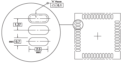 However, in 2001 CAD vendors started to add Rounded Rectangle pad shape as an option. It was a marketing concept, and they claimed that rounded rectangle pad shape was best for lead-free solder, but they never explained why. The rounded rectangle pad shape was a trade off between rectangle and oblong. The reason to move away from rectangle pad shape was because the paste mask stencil used lasers to cut aperture openings and the aperture corners were rounded. Also, assembly shops had issues with rectangular apertures and new lead-free solder alloys sticking in the corners during the stencil release. To solve this problem, they experimented with rounded corner apertures and had better stencil release results. Laser Cut Paste Mask Stencil: 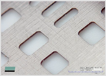 Even if the PCB library uses rectangle pad shapes, the paste mask stencil apertures still have rounded corners. Thus, no paste mask in the pad corners. The left image is lead solder. Right is lead-free solder. 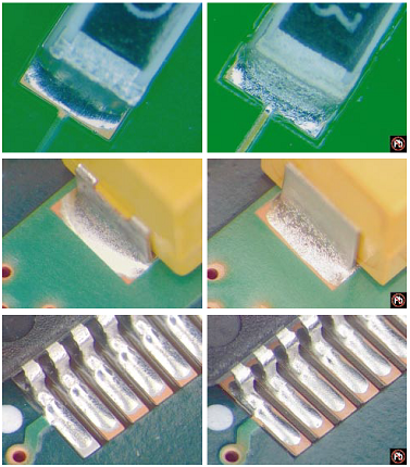 It didn’t take long before the rounded rectangle pad shape became popular. The paste mask stencil manufacturer could use the rounded rectangle pad shape to achieve full paste mask coverage on the pad and achieve the best paste mask stencil release. The biggest question is how much corner radius is good and does making it too big cause problems. The best solution is to establish a corner radius percentage of the pad width and have a corner radius limit. The smaller the pad width and smaller the corner radius. The most important issue is that the component package terminal lead must reside 100% on the pad. The ideal situation is not to have a metal terminal lead corner hanging off the rounded cornered pad in an area that has no solder mask. 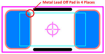 Another advantage of rounded rectangle pad shape is RF PCB layout. RF designs perform better by avoiding square corner copper features for pads, traces and copper pour. Many terminal leads are rectangular shaped, so the corner rounding should be modest. 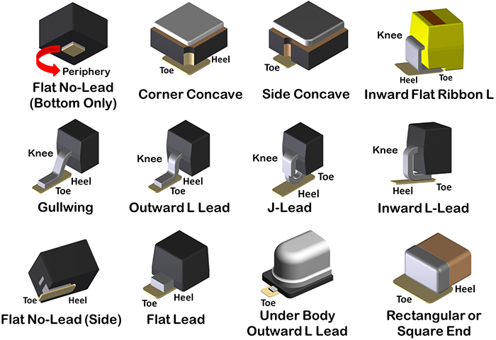  PCB Footprint Expert Simplify your PCB design process with the Footprint Expert, the ultimate tool for ensuring optimal solder pad shapes and layout precision. Whether you’re working with popular Surface Mount footprint shapes like Rectangle, Rounded Rectangle, Oblong, or D-Shape, the Footprint Expert automates solder mask calculations, ensuring compliance with fabrication rules such as minimum solder mask web and swell. It helps you optimize pad shapes like the rounded rectangles, among other (not to mention the 3D STEP models!). The Footprint Expert ensures that pads align perfectly with component terminals, enhancing both reliability and RF performance. Get your FREE Footprint Calculator or Footprint Expert Evaluation License:
|
|
 |
|
 |
|
Post Reply 
|
|
| Tweet |
| Forum Jump | Forum Permissions  You cannot post new topics in this forum You cannot reply to topics in this forum You cannot delete your posts in this forum You cannot edit your posts in this forum You cannot create polls in this forum You cannot vote in polls in this forum |