
 |

|
Land Patterns For Lead-Free Componet Soldering |
Post Reply 
|
| Author | |
poojangarg 
New User 
Joined: 15 Oct 2012 Location: India Status: Offline Points: 4 |
 Post Options Post Options
 Thanks(0) Thanks(0)
 Quote Quote  Reply Reply
 Topic: Land Patterns For Lead-Free Componet Soldering Topic: Land Patterns For Lead-Free Componet SolderingPosted: 15 Oct 2012 at 10:00pm |
|
Hi All,
Is there any standard that we should follow for land patterns for Pb-Free componet soldering?
Thanks
Poojan
|
|
 |
|
 |
|
muthu 
Active User 
Joined: 20 Aug 2012 Location: kovai Status: Offline Points: 27 |
 Post Options Post Options
 Thanks(2) Thanks(2)
 Quote Quote  Reply Reply
 Posted: 25 Oct 2012 at 5:34am Posted: 25 Oct 2012 at 5:34am |
|
the IPC7351-B is using rounded rectangle pad shape for many components,
even the chip. Rounded pads are better for lead-free surface mount
assembly using reflow, because lead-free solder doesn't flow as well as
leaded solder and the aperture openings in the paste mask stencil are
rounded corners. It may also benefit low profile components since it
reduces the paste used.
 |
|
 |
|
Tom H 
Admin Group 

Joined: 05 Jan 2012 Location: San Diego, CA Status: Offline Points: 5719 |
 Post Options Post Options
 Thanks(1) Thanks(1)
 Quote Quote  Reply Reply
 Posted: 25 Oct 2012 at 10:48am Posted: 25 Oct 2012 at 10:48am |
|
Rounded Rectangular pad shape will eventually take over as the only Pad Shape for SMT (BGA's are the exception).
No more Rectangle, Oblong, D-Shape or Square, just Rounded Rectangle. It will take some time but eventually it will be the global universal standard. |
|
 |
|
poojangarg 
New User 
Joined: 15 Oct 2012 Location: India Status: Offline Points: 4 |
 Post Options Post Options
 Thanks(0) Thanks(0)
 Quote Quote  Reply Reply
 Posted: 25 Oct 2012 at 9:51pm Posted: 25 Oct 2012 at 9:51pm |
|
But how does rouneded rectangle helps in lead-free soldering so far whatever I had have read on internet is that it is manufacturing process that dictates lead-free soldering.
|
|
 |
|
jameshead 
Expert User 
Joined: 20 Mar 2012 Location: Oxfordshire, UK Status: Offline Points: 576 |
 Post Options Post Options
 Thanks(1) Thanks(1)
 Quote Quote  Reply Reply
 Posted: 26 Oct 2012 at 1:23am Posted: 26 Oct 2012 at 1:23am |
|
Ignoring solder paste aperture size and just looking at the copper pad alone I don't think that rounded rectangles are any better or worse then a normal rectangle for lead-free solder then leaded solder.
But because the viscosity of lead-free solder is different then the solder doesn't run out all the way to the corners of a rectangle pad so it's wasted copper that you may as well as eliminate by using a rounded corner. The rounded corner has the advantage in that it gives you that little bit more space for routing tracks, at a 45 degree angle, next to the pad. This is what I've picked up anyway by talking to a few people. I've not looked in depth at it. |
|
 |
|
poojangarg 
New User 
Joined: 15 Oct 2012 Location: India Status: Offline Points: 4 |
 Post Options Post Options
 Thanks(0) Thanks(0)
 Quote Quote  Reply Reply
 Posted: 26 Oct 2012 at 4:06am Posted: 26 Oct 2012 at 4:06am |
|
Solder paste size can be controlled at both PCB design and manufacturing stage for that I don't think we need to modify complete pad structure.
I am asking so much questions because in our organisation we have been facing soldering problem and we are suppose to resolve all the issues either it is at design stage or at manufacturing and we need to prepare a doument for that. So any further help in this thread or through document will be very grateful. |
|
 |
|
Tom H 
Admin Group 

Joined: 05 Jan 2012 Location: San Diego, CA Status: Offline Points: 5719 |
 Post Options Post Options
 Thanks(0) Thanks(0)
 Quote Quote  Reply Reply
 Posted: 26 Oct 2012 at 7:04am Posted: 26 Oct 2012 at 7:04am |
|
All pad shapes are Lead-Free. The pad shape has nothing to do with Lead-Free.
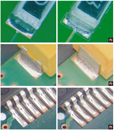
The Rounded Rectangle Pad Shape is excellent for both Lead and Lead-Free solder. Solder Paster is applied over the entire pad with a Stencil that has aperture openings that where cut out using a laser. The laser does not create sharp corners but rather the corners of a rectangle pad shape are slighty rounded in the Paste Mask Stencil. When the PCB goes through the reflow oven, the paste mask melts and moves toward the component lead. The solder in the pad corners disappears. This happens on every surface mount pad for SOP, QFP, Molded Body, Chip, PLCC and other component families. Here is a top view picture of Chip Resistor on the top 2 pictures, Molded Body tantalum capacitors on the middle 2 pictures, SOP in the bottom 2 pictures and you can clearly see that after the reflow oven, there is no solder in the pad corners. The left side pictures are Lead solder and the right side is Lead Free Solder.  |
|
 |
|
Post Reply 
|
|
| Tweet |
| Forum Jump | Forum Permissions  You cannot post new topics in this forum You cannot reply to topics in this forum You cannot delete your posts in this forum You cannot edit your posts in this forum You cannot create polls in this forum You cannot vote in polls in this forum |