
 |

|
Class A (Most) Land Pattern Extended Pads |
Post Reply 
|
| Author | |
Alex Quilty 
New User 
Joined: 20 May 2024 Status: Offline Points: 4 |
 Post Options Post Options
 Thanks(0) Thanks(0)
 Quote Quote  Reply Reply
 Topic: Class A (Most) Land Pattern Extended Pads Topic: Class A (Most) Land Pattern Extended PadsPosted: 11 Jun 2024 at 7:28am |
|
Hey everyone,
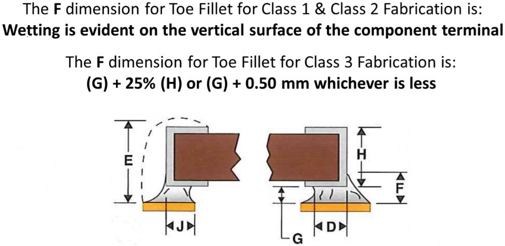
My understanding for IPC's Class A Land Patterns is that they perform just as well as Class B (Nominal) Land Patterns. I also know that the Class A Land Patterns have been kept for those who may be soldering the component to the PCB by hand. Finally, where I am a little confused, is where a particular Pad may be too small or too big, this could cause issues in manufacturing to IPC Class specifications depending on the size, which leads me to the question: Is it okay to extend my Pads to allow for easier hand soldering? If so, how much longer am I allowed to make these Pads before it degrades the Fillet too much, since the solder would be spreading along the Pad instead of climbing the lead to form the Filet? Edit: I just noticed the Land Pattern Forum section, I can move this there if you would like, otherwise I will leave it here, or if a MOD could move this post, that would be awesome! Let me know if you want me to move it. |
|
 |
|
 |
|
Tom H 
Admin Group 

Joined: 05 Jan 2012 Location: San Diego, CA Status: Offline Points: 5719 |
 Post Options Post Options
 Thanks(1) Thanks(1)
 Quote Quote  Reply Reply
 Posted: 11 Jun 2024 at 8:30am Posted: 11 Jun 2024 at 8:30am |
|
You can't manually solder BTC or Grid Array parts, and Gullwing parts don't require a lot of solder on the Toe.  |
|
 |
|
Post Reply 
|
|
| Tweet |
| Forum Jump | Forum Permissions  You cannot post new topics in this forum You cannot reply to topics in this forum You cannot delete your posts in this forum You cannot edit your posts in this forum You cannot create polls in this forum You cannot vote in polls in this forum |