
 |

|
To Neck or Not to Neck, That is the Question |
Post Reply 
|
| Author | |
NeilVPeers 
Active User 
Joined: 04 Aug 2016 Status: Offline Points: 17 |
 Post Options Post Options
 Thanks(0) Thanks(0)
 Quote Quote  Reply Reply
 Topic: To Neck or Not to Neck, That is the Question Topic: To Neck or Not to Neck, That is the QuestionPosted: 01 Dec 2016 at 5:46am |
|
I would appreciate other peoples' view of whether traces should be necked down (or not) when entering a SMD pad and what percentage of the pad width is the trace width allowed to be.
Is it best practice, recommended practice or do it if you think it will benefit the assembly? I am assuming necking down is to minimise heatloss from the pad when soldering. Is this relevant if the whole board is being preheated? Many thanks Neil
|
|
 |
|
 |
|
Tom H 
Admin Group 

Joined: 05 Jan 2012 Location: San Diego, CA Status: Offline Points: 5718 |
 Post Options Post Options
 Thanks(0) Thanks(0)
 Quote Quote  Reply Reply
 Posted: 01 Dec 2016 at 8:20am Posted: 01 Dec 2016 at 8:20am |
|
What trace width are you using on the outer layers for VCC, GND and other voltages?
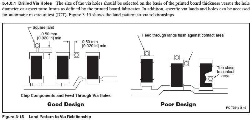
I've been involved in over 2,000 PCB design layouts over the past 40 years and never neck down wide traces. You might think that large traces might conduct heat away from the solder joint producing a cold solder joint. But I learned back in 1982 from senior PCB designers that a cold solder joint can only be produced by a copper area larger than the size of a USA Quarter $0.25 - 0.955 inches (24.26 mm). I need to know what your problem is and why you have to neck down. Is it because the IPC-7351B Standard has this illustration?  |
|
 |
|
NeilVPeers 
Active User 
Joined: 04 Aug 2016 Status: Offline Points: 17 |
 Post Options Post Options
 Thanks(0) Thanks(0)
 Quote Quote  Reply Reply
 Posted: 02 Dec 2016 at 2:52am Posted: 02 Dec 2016 at 2:52am |
|
The question has arisen owing to our PCB tool (Altium) having it as an optional design check. That and the pad sizes on the smaller components now combined with the worry of heat being sucked out of them. I am, however, reassured by your comment on that.
As an example I am using a TPS2546 and setting a current limit of 2A. With the temperature rise constraints and the layer stack, the trace width required is a minimum 0.35mm. The pad on the device is only 0.26mm wide. The impedance requirements for the data traces on the same device calls for a trace 0.381mm wide, also going to pads that are also only 0.26mm wide. Consequently some neck down has to occur otherwise adjacent pads get shorted. This also raised the question of "heat sucking" and hence the question of what neck down value should be used. |
|
 |
|
Matthew Lamkin 
Advanced User 
Joined: 02 Oct 2012 Status: Offline Points: 284 |
 Post Options Post Options
 Thanks(0) Thanks(0)
 Quote Quote  Reply Reply
 Posted: 20 Dec 2016 at 4:07am Posted: 20 Dec 2016 at 4:07am |
|
So the standards themselves recommend necking down.
Then isn't it time the standards were updated and this changed? TBH I think that this is something that needs considering on a net by net, pad by pad - connection basis. Each joint having it's own requirements i.e. if impedance controlled or if a big fat track going into an 0201 and you use a poor assembler :) |
|
 |
|
Tom H 
Admin Group 

Joined: 05 Jan 2012 Location: San Diego, CA Status: Offline Points: 5718 |
 Post Options Post Options
 Thanks(0) Thanks(0)
 Quote Quote  Reply Reply
 Posted: 15 May 2017 at 6:38pm Posted: 15 May 2017 at 6:38pm |
|
The 7351 standard is way out of date. Almost every page needs to be updated. IPC updated the CID and CID+ study guide and test, but valuable standards go on unfinished. Out of the original 7351 creators from 2001 Dieter Bergman (deceased), Gary Ferrari (retired), John Perry (promoted to Director), Karen McConnell (busy at NGC as CAD manager), and myself, I am the only one left contributing. Karen hosts a bi-weekly meetings every other Wednesday and the 7351 standard is stalled in committee. The IPC Liaison that replaced Dieter is off on another project. |
|
 |
|
Post Reply 
|
|
| Tweet |
| Forum Jump | Forum Permissions  You cannot post new topics in this forum You cannot reply to topics in this forum You cannot delete your posts in this forum You cannot edit your posts in this forum You cannot create polls in this forum You cannot vote in polls in this forum |