

|
|
0402 Capacitors Under 1 mm Pitch BGA |
Post Reply 
|
| Author | |
DaveCowl 
Advanced User 

Joined: 18 Oct 2012 Location: Santa Clara, CA Status: Offline Points: 161 |
 Post Options Post Options
") Thanks(0) Thanks(0)
 Quote Reply Quote Reply
 Topic: 0402 Capacitors Under 1 mm Pitch BGA Topic: 0402 Capacitors Under 1 mm Pitch BGAPosted: 26 Nov 2012 at 3:31pm |
|
I know that it is possible to have 0402 parts under the via breakout for a 1mm BGA. I am currently pondering how best to do this. Right now I have s60r12 pads with v50h25 vias, and Expedition is nudging the vias slightly, indicating that I have cut things just a little too close. I could do any of the following to fix this: 1) Smaller square pad (or go to Least Material rather than Nominal). 2) Reduce the clearance requirement 3) Larger radius making the pad more round 4) Smaller via pad and possibly hole My resistor pads are actually slightly bigger again (r64_63r13) so they will need a little more of whatever is the best approach... Ideally I would like to just have one 0402 cap footprint and one 0402 res footprint in the layout, but it would also be possible to have two of each, wuth a special one for under the BGA. Any thoughts on this appreciated.
|
|
 |
|
|
|
|
DaveCowl
Advanced User
Joined: 18 Oct 2012 Location: Santa Clara, CA Status: Offline Points: 161 |
Post Options
Thanks(0)
Quote Reply
Posted: 26 Nov 2012 at 3:32pm |
|
I guess a fifth option is to tolerate the vias being shifted slightly off grid... though this might be more problematic with the resistors when I try to place those as is... |
|
|
|
|
Tom H
Admin Group 

Joined: 05 Jan 2012 Location: San Diego, CA Status: Offline Points: 5716 |
Post Options
Thanks(0)
Quote Reply
Posted: 26 Nov 2012 at 5:01pm |
|
Turn on Rounded Rectangle pad shape for the 0402.
Here is a 1 mm pitch BGA with dogbone fanout. The 0402 can be perfect center via-in-pad or located in-between fanout vias if there's room.  I would go for the via-in-pad with plugged via. You can see where the Rounded Rectangle pad shape passes DRC clearance checks. Cap the via-in-pad with surface finish, planerize flat and ready for reflow with BGA fanout on one side and capacitor pad on the other side.  With capacitors, a small "dimple" (with trapped air) in the pad would not create a void cavity in the lead like they do in BGA via-in-pad. 25% void is acceptable. 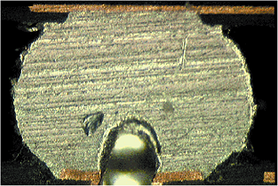 |
|
|
|
|
DaveCowl
Advanced User
Joined: 18 Oct 2012 Location: Santa Clara, CA Status: Offline Points: 161 |
Post Options
Thanks(0)
Quote Reply
Posted: 26 Nov 2012 at 5:28pm |
|
I think that they will fit with the Least Material selected - that brings the pad down to s50r10. I also imagine that via in pad will cause a stir for the folks who see any added process to the PCB as expensive (even though we will have $400 FPGAs on these boards...). But I can see if it will fly. Thanks!
|
|
|
|
|
Post Reply
|
|
| Tweet |
| Forum Jump | Forum Permissions You cannot post new topics in this forum You cannot reply to topics in this forum You cannot delete your posts in this forum You cannot edit your posts in this forum You cannot create polls in this forum You cannot vote in polls in this forum |


 Topic Options